
搜索到
1
篇与
的结果
-
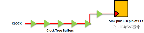
 博文速递:Clock Gating VLSI SoC Design IP与SoC设计 2022年05月09日 12:10 江苏Clock GatingClock signal is the highest frequency toggling signal in any SoC. As we discussed in the post: Need for Low-Power Design Methodology, the capacitive load power component of the dynamic power is directly proportional to the switching frequency of the devices. This implies that clock path cells would contribute maximum to the dynamic power consumption in the SoC. Power consumption in the clock paths alone contribute to more than 50% of the total dynamic power consumed within modern SoCs. Power being a very critical aspect of the design, one needs to make prudent efforts to reduce this. Clock Gating is one such method. Let's try and build further on this perspective.Clock feeds the CLOCK pins all the Flip-Flops in the design. Clock Tree itself comprises of clock tree buffers which are needed to maintain a sharp slew (numerically small) in the clock path. Refer to the post Clock Transition for details. Consider the above figure. It is not necessary that the output of the flip-flop would be switching at all times. Modern devices support various low-power modes in which only a certain part of your SoC is working. This may include some key features pertaining to security or some critical functional aspects of your device. Apart from this, there are some configuration registers in your device which need to be programmed either once or very seldom. So, let's say, the above FF will not be switching states for a considerable period of time. If it is used the way it is, what's the problem? Power! Clock is switching incessantly. Clock Tree buffers are switching states and hence consuming power. So are the FFs. Remember that FF itself is made up of latches. So, despite the fact that input and output of the FF is not switching, some part of the latch is switching and consuming power.What could be done to alleviate the above problem? Clock Gating is one such solution. Here's how it'll help.If you place an AND gate at the clock path and knowing that you don't need a certain part of your device to receive clock, drive a logic '0' on the ENABLE pin. This would ensure that all the Clock Tree buffers and the sink pin of the FF are held at a constant value (0 in this case). Hence these cells would not contribute to dynamic power dissipation. However, they would still consume leakage power.Similarly, you can place an OR gate and drive it's one input to logic 1. Again, you would save on the dynamic power.However, a word of caution. The output of the AND gate feeding the entire clock path might be glitchy. See the following figure:Solution: The output won't be glitchy if the enable signal changes only when the CLOCK signal is low. So, all you gotta make sure is that ENABLE is generated by a negative-edge triggered FF. This would ensure that the signal is changing after the fall edge of the CLOCK signal.Similarly, while using an OR-gate, clock pulse would be propagated if the ENABLE signal changes when the CLOCK is high. Make sure that it is generated by a positive-edge triggered FF in order to avoid any glitch being passed onto the FFs. Why would a glitch be detrimental anyway? The answer is:Glitches constitute an edge! FF might sample the value because they are edge-triggered. But, problem is that all FFs have a certain duty cycle requirement (Also called Pulse-width check), which needs to be fulfilled in order to ensure that they don't go into METASTABILITY. And if an unknown state : X is propagated in a design, the entire functionality of the chip can go haywire!Some terminologies: •AND/NAND gate based clock gating is referred to as Active-High Clock Gating. •OR/NOR gate based clock gating is referred to as Active-Low Clock Gating.NAND and NOR clock gates work similar to AND and OR respectively.So, Clock Gating is an efficient solution to save dynamic power consumption in the design. Modern SoCs have many IPs integrated together. Placing a clock gate and enabling them in various possible combinations is what gives rise to different low-power modes in the device.If any content of this article infringes, please contact us to remove this article.来自微信