
搜索到
25
篇与
的结果
-
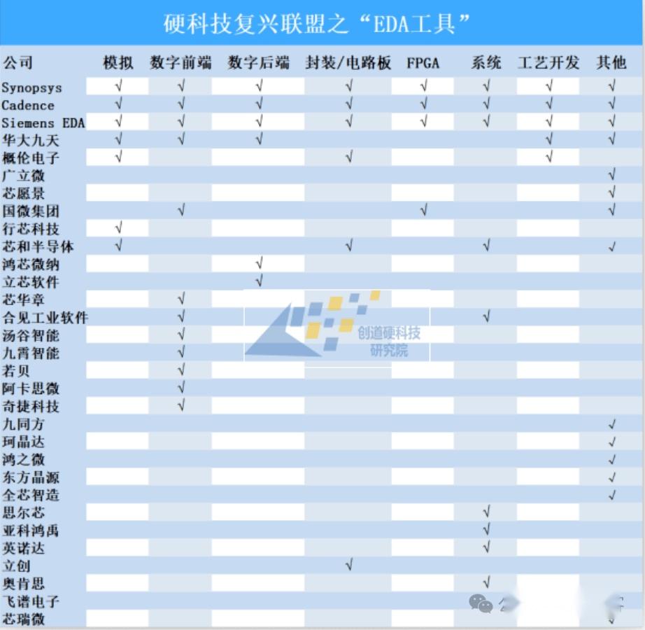
 国产EDA工具厂商汇总与世界三大巨头对比 从国内EDA市场来看,美国三大EDA厂商也占据了主导地位。根据赛迪智库数据显示,2020年Synopsys、Cadence和Seimens EDA三巨头合计占领国内约80%的市场份额,国产EDA厂商的份额仅11.5%,其中华大九天占据了国内EDA市场约6%的市场份额,居本土EDA企业首位。近年来,全球 EDA 市场呈现出稳步增长的态势。根据市场研究机构的数据,2020-2025 年期间,全球 EDA 市场规模持续攀升(见下图 )。2020 年,全球 EDA 市场规模约为 115 亿美元,到 2025 年,预计将达到 157 亿美元,年均复合增长率为 6.4%。这一增长主要得益于 5G、AI、物联网等新兴技术的快速发展,以及全球范围内对高性能、低功耗芯片的需求不断增加。
 -
SV中inout与ref区别 一、Inout是什么?inout百度翻译为“双向,双向总线”,顾名思义就是该类型端口既能做输入又能做输出。很多需要交互的芯片外部的有些管脚都会使用inout类型,尤其是需要与外界做双向通信的数据总线与地址总线。在需要用到inout类型搭建仿真验证平台时,需要注意以下两个方面:1.在例化端口时,需将顶层的inout型的信号必须变为wire型;2.在编写assign语句时,其必须放在initial或always块外部。想对inout型的信号进行读写操作时需使用assign语句,具体代码如下:module TB(); wire data_inout; reg data_reg; reg db_link; initial begin .......... end assign data_inout = db_link ? data_reg : 1'hz; endmodule二、Ref是什么?Ref为Reference的缩写,百度翻译为“参考,引用”。通过查阅资料,ref类型会使参数按照引用传递。下面为本人在验证工作时碰到的一个例子:设计(DUT)源程序部分代码:module DUT; endmodule验证环境 (Test_Bench—cpu_mod) 部分代码:`timescale 1ns/1ps module cpu_mod; parameter cpu_period = 33.33; parameter cpu_period*2 = 66.67; parameter cpu_period*9 = 299.97; initial begin write_flag = 0; end task automatic cpu_write (input [15:0] addr , input [15:0] data , ref logic cs); dut.if.ebi_rd_wr = 1'b1; cs = 1 ; #cpu_period; dut.if.ebi_addr = addr ; dut.if.ebi_rd_wr = 1'b0 ; dut.if.ebi_ts = 1'b0 ; cs = 0 ; #cpu_period*2; dut.if.ebi_ts = 1'b1 ; write_flag = 1 ; cpu_wdata = data ; dut.if.ebi_we_be0 = 1'b0 ; dut.if.ebi_we_be1 = 1'b0 ; #cpu_period*9; dut.if.ebi_rd_wr = 1'b1 ; dut.if.ebi_we_be0 = 1'b1 ; dut.if.ebi_we_be1 = 1'b1 ; #cpu_period; write_flag = 0 ; dut.if.ebi_addr = 16'hz ; cpu_wdata = 16'h0 ; cs = 1 ; endtask endmodule测试用例 (Test_Case) 部分代码:`timescale 1ns/1ps module testcase(interface dut_if); bit [15:0] cpu_addr1 = 16'h1803; bit [15:0] cpu_data1 = 16'h1234; initial begin #150ms; cpu_mod.cpu_write (cpu_addr1,cpu_data1,dut_if.ebi_cs3); end endmodule 1)代码结构的思路待更新2)代码结构的说明待更新三、两者区别是什么?当task和function的形式参数被声明为input类型时,input类型的形参只是进行了数值的拷贝;而当task和function的形式参数被声明为output类型时,output类型的形参会在return时刻将数值拷贝至接收方。这就不难得出 inout 类型不仅会在输入时进行数值的拷贝,而且会在输出时将数值拷贝至接收方。Ref 类型的形参,我们做的不是拷贝,而是 引用 。对于task来讲,ref类型的参数,其外部是可见的,换句话说在外部对ref的形参数值进行的修改,task是可见且同步变化的;而inout类型的参数,task得到的仅仅是一个拷贝过来的数值,在整个task运行期间,外部的数值无论发生什么变化,对于task而言是未知的,同理task对该数值在其内部进行的修改,只有task运行结束后,外部才会获得该值。四、两者联系/区别总结Inout 与 Ref 均可以在task与function中传入传出数据;Inout 在外部传递的参数改变时,其调用的task或function无法实时更新,只有当调用的task或function执行完毕后才会发生变化;Ref 在外部传递的参数改变时,其调用的task或function能够实时更新数值;Ref 操作不需要消耗仿真时间,而 Inout 则需要消耗仿真时间。————————————————版权声明:本文为CSDN博主「进击的砰砰砰」的原创文章,遵循CC 4.0 BY-SA版权协议,转载请附上原文出处链接及本声明。原文链接:https://blog.csdn.net/weixin_42493102/article/details/122311686
-
Yosys工具概述 对于一个新工具,以及学习源码,可以让ai帮忙分析。例如下面源码解读使用的kimi协助分析 一、基本使用【从零开始学习VLSI设计(一)】Yosys工具概述-CSDN博客1.安装$ sudo apt-get install build-essential clang bison flex libreadline-dev gawk tcl-dev libffi-dev git graphviz xdot pkg-config python3 libboost-system-dev libboost-python-dev libboost-filesystem-dev zlib1g-dev $ git clone https://github.com/YosysHQ/yosys.git $ cd yosys $ make $ sudo make install2.使用//读取top.v read_verilog top.v //读取lib库 read_verilog -lib -specify +/xilinx/cells_sim.v read_verilog -lib +/xilinx/cells_xtra.v //检查层次连接 hierarchy -check -auto-top //综合 synth_xilinx -flatten -nosrl -noclkbuf -nodsp //显示连接关系图 show //执行优化 opt二、项目结构Yosys 是一个开源的硬件描述语言(HDL)合成工具,它主要用于将 Verilog 或 VHDL 代码转换成门级网表(netlist),这些网表可以被发送到 ASIC 或 FPGA 的合成工具。Yosys 支持多种不同的后端目标,使其成为一个灵活的前端合成工具。Yosys 的项目结构大致如下:内核(Kernel)包含 Yosys 的核心功能,如内存管理、日志记录、基本数据类型和算法等。前端(Frontends)用于读取和解析不同的硬件描述语言,如 Verilog、VHDL、SystemVerilog 等。将 HDL 代码转换成 Yosys 内部表示(AST - Abstract Syntax Tree)。后端(Backends)用于将 Yosys 内部表示转换成不同的网表格式,如 EDIF、Bels、Netlists 等。支持多种不同的技术目标,如 Xilinx、Altera/Intel、Lattice 等。优化(Optimizations)包含一系列优化传递(passes),用于改进和简化内部表示。优化包括但不限于常数传播、死代码消除、代数简化、查找表优化等。库(Libraries)提供了一系列预定义的逻辑单元(如 LUTs、Flip-Flops、内存单元等)和宏单元。用于生成特定功能的标准单元和宏。工具(Tools)提供了一系列用于调试、分析和转换设计的工具。包括查看器、测试生成器、等价性检查器等。测试(Tests)包含了用于测试 Yosys 功能的自动化测试套件。用于确保 Yosys 的功能正确性和稳定性。文档(Documentation)提供了用户手册、内部 API 文档和开发文档。帮助用户和开发者理解如何使用和贡献 Yosys。脚本和示例(Scripts and Examples)提供了一系列示例和脚本,展示如何使用 Yosys 进行不同的合成和优化任务。用于教学和作为最佳实践的参考。第三方集成(Third-party Integrations)包括与第三方工具链的集成,如 OpenSTA、ABC 等。提供了与这些工具的接口,以便在合成流程中使用它们的特定功能。Yosys 的项目结构设计得既模块化又可扩展,使得它可以适应不同的用户需求和目标平台。开发者可以通过添加新的前端、后端或优化传递来扩展 Yosys 的功能。三、内部数据结构上图为yosys内部的逻辑门类型 上图为yosys内部网表的主要数据结构 以下是 rtlil.h 和 rtlil.cc 文件中与 design->modules() 相关的一些关键点:RTLIL::Design 类:定义了 RTLIL::Design 类,它表示整个设计,包含所有模块和其他全局信息。RTLIL::Design 类中有一个 modules 成员,它是一个 std::vector,存储设计中的所有模块。RTLIL::Module 类:定义了 RTLIL::Module 类,它表示设计中的一个模块,是设计的基本构建块。RTLIL::Module 类包含成员如 wires、cells 等,用于存储模块内的线网和单元。RTLIL::Wire 类:定义了 RTLIL::Wire 类,它表示一个线网,用于连接模块内的信号。RTLIL::Cell 类:定义了 RTLIL::Cell 类,它表示一个单元,如逻辑门或存储元件。RTLIL::SigSpec 类:定义了 RTLIL::SigSpec 类,它表示一个信号规范,可以包含多个信号位或信号块。RTLIL::SigBit 类:定义了 RTLIL::SigBit 类,它表示一个信号位,可以是一个线网的一部分或一个常量值。这些数据结构共同构成了 Yosys 处理和存储网表信息的基础设施。通过这些数据结构,Yosys 可以读取、修改和输出 RTL 级别的硬件设计。RTLIL::Designstruct RTLIL::Design { unsigned int hashidx_; unsigned int hash() const { return hashidx_; } pool<RTLIL::Monitor*> monitors; dict<std::string, std::string> scratchpad; bool flagBufferedNormalized = false; void bufNormalize(bool enable=true); int refcount_modules_; dict<RTLIL::IdString, RTLIL::Module*> modules_; std::vector<RTLIL::Binding*> bindings_; std::vector<AST::AstNode*> verilog_packages, verilog_globals; std::unique_ptr<define_map_t> verilog_defines; std::vector<RTLIL::Selection> selection_stack; dict<RTLIL::IdString, RTLIL::Selection> selection_vars; std::string selected_active_module; Design(); ~Design(); RTLIL::ObjRange<RTLIL::Module*> modules(); RTLIL::Module *module(const RTLIL::IdString &name); const RTLIL::Module *module(const RTLIL::IdString &name) const; RTLIL::Module *top_module(); bool has(const RTLIL::IdString &id) const { return modules_.count(id) != 0; } void add(RTLIL::Module *module); void add(RTLIL::Binding *binding); RTLIL::Module *addModule(RTLIL::IdString name); void remove(RTLIL::Module *module); void rename(RTLIL::Module *module, RTLIL::IdString new_name); void scratchpad_unset(const std::string &varname); void scratchpad_set_int(const std::string &varname, int value); void scratchpad_set_bool(const std::string &varname, bool value); void scratchpad_set_string(const std::string &varname, std::string value); int scratchpad_get_int(const std::string &varname, int default_value = 0) const; bool scratchpad_get_bool(const std::string &varname, bool default_value = false) const; std::string scratchpad_get_string(const std::string &varname, const std::string &default_value = std::string()) const; void sort(); void check(); void optimize(); bool selected_module(const RTLIL::IdString &mod_name) const; bool selected_whole_module(const RTLIL::IdString &mod_name) const; bool selected_member(const RTLIL::IdString &mod_name, const RTLIL::IdString &memb_name) const; bool selected_module(RTLIL::Module *mod) const; bool selected_whole_module(RTLIL::Module *mod) const; RTLIL::Selection &selection() { return selection_stack.back(); } const RTLIL::Selection &selection() const { return selection_stack.back(); } bool full_selection() const { return selection_stack.back().full_selection; } template<typename T1> bool selected(T1 *module) const { return selected_module(module->name); } template<typename T1, typename T2> bool selected(T1 *module, T2 *member) const { return selected_member(module->name, member->name); } template<typename T1> void select(T1 *module) { if (selection_stack.size() > 0) { RTLIL::Selection &sel = selection_stack.back(); sel.select(module); } } template<typename T1, typename T2> void select(T1 *module, T2 *member) { if (selection_stack.size() > 0) { RTLIL::Selection &sel = selection_stack.back(); sel.select(module, member); } } std::vector<RTLIL::Module*> selected_modules() const; std::vector<RTLIL::Module*> selected_whole_modules() const; std::vector<RTLIL::Module*> selected_whole_modules_warn(bool include_wb = false) const; #ifdef WITH_PYTHON static std::map<unsigned int, RTLIL::Design*> *get_all_designs(void); #endif };RTLIL::Modelstruct RTLIL::Module : public RTLIL::AttrObject { unsigned int hashidx_; unsigned int hash() const { return hashidx_; } protected: void add(RTLIL::Wire *wire); void add(RTLIL::Cell *cell); void add(RTLIL::Process *process); public: RTLIL::Design *design; pool<RTLIL::Monitor*> monitors; int refcount_wires_; int refcount_cells_; dict<RTLIL::IdString, RTLIL::Wire*> wires_; dict<RTLIL::IdString, RTLIL::Cell*> cells_; std::vector<RTLIL::SigSig> connections_; std::vector<RTLIL::Binding*> bindings_; RTLIL::IdString name; idict<RTLIL::IdString> avail_parameters; dict<RTLIL::IdString, RTLIL::Const> parameter_default_values; dict<RTLIL::IdString, RTLIL::Memory*> memories; dict<RTLIL::IdString, RTLIL::Process*> processes; Module(); virtual ~Module(); virtual RTLIL::IdString derive(RTLIL::Design *design, const dict<RTLIL::IdString, RTLIL::Const> ¶meters, bool mayfail = false); virtual RTLIL::IdString derive(RTLIL::Design *design, const dict<RTLIL::IdString, RTLIL::Const> ¶meters, const dict<RTLIL::IdString, RTLIL::Module*> &interfaces, const dict<RTLIL::IdString, RTLIL::IdString> &modports, bool mayfail = false); virtual size_t count_id(const RTLIL::IdString& id); virtual void expand_interfaces(RTLIL::Design *design, const dict<RTLIL::IdString, RTLIL::Module *> &local_interfaces); virtual bool reprocess_if_necessary(RTLIL::Design *design); virtual void sort(); virtual void check(); virtual void optimize(); virtual void makeblackbox(); void connect(const RTLIL::SigSig &conn); void connect(const RTLIL::SigSpec &lhs, const RTLIL::SigSpec &rhs); void new_connections(const std::vector<RTLIL::SigSig> &new_conn); const std::vector<RTLIL::SigSig> &connections() const; std::vector<RTLIL::IdString> ports; void fixup_ports(); pool<pair<RTLIL::Cell*, RTLIL::IdString>> bufNormQueue; void bufNormalize(); template<typename T> void rewrite_sigspecs(T &functor); template<typename T> void rewrite_sigspecs2(T &functor); void cloneInto(RTLIL::Module *new_mod) const; virtual RTLIL::Module *clone() const; bool has_memories() const; bool has_processes() const; bool has_memories_warn() const; bool has_processes_warn() const; std::vector<RTLIL::Wire*> selected_wires() const; std::vector<RTLIL::Cell*> selected_cells() const; template<typename T> bool selected(T *member) const { return design->selected_member(name, member->name); } RTLIL::Wire* wire(const RTLIL::IdString &id) { auto it = wires_.find(id); return it == wires_.end() ? nullptr : it->second; } RTLIL::Cell* cell(const RTLIL::IdString &id) { auto it = cells_.find(id); return it == cells_.end() ? nullptr : it->second; } const RTLIL::Wire* wire(const RTLIL::IdString &id) const{ auto it = wires_.find(id); return it == wires_.end() ? nullptr : it->second; } const RTLIL::Cell* cell(const RTLIL::IdString &id) const { auto it = cells_.find(id); return it == cells_.end() ? nullptr : it->second; } RTLIL::ObjRange<RTLIL::Wire*> wires() { return RTLIL::ObjRange<RTLIL::Wire*>(&wires_, &refcount_wires_); } RTLIL::ObjRange<RTLIL::Cell*> cells() { return RTLIL::ObjRange<RTLIL::Cell*>(&cells_, &refcount_cells_); } void add(RTLIL::Binding *binding); // Removing wires is expensive. If you have to remove wires, remove them all at once. void remove(const pool<RTLIL::Wire*> &wires); void remove(RTLIL::Cell *cell); void remove(RTLIL::Process *process); void rename(RTLIL::Wire *wire, RTLIL::IdString new_name); void rename(RTLIL::Cell *cell, RTLIL::IdString new_name); void rename(RTLIL::IdString old_name, RTLIL::IdString new_name); void swap_names(RTLIL::Wire *w1, RTLIL::Wire *w2); void swap_names(RTLIL::Cell *c1, RTLIL::Cell *c2); RTLIL::IdString uniquify(RTLIL::IdString name); RTLIL::IdString uniquify(RTLIL::IdString name, int &index); RTLIL::Wire *addWire(RTLIL::IdString name, int width = 1); RTLIL::Wire *addWire(RTLIL::IdString name, const RTLIL::Wire *other); RTLIL::Cell *addCell(RTLIL::IdString name, RTLIL::IdString type); RTLIL::Cell *addCell(RTLIL::IdString name, const RTLIL::Cell *other); RTLIL::Memory *addMemory(RTLIL::IdString name, const RTLIL::Memory *other); RTLIL::Process *addProcess(RTLIL::IdString name); RTLIL::Process *addProcess(RTLIL::IdString name, const RTLIL::Process *other); // The add* methods create a cell and return the created cell. All signals must exist in advance. RTLIL::Cell* addNot (RTLIL::IdString name, const RTLIL::SigSpec &sig_a, const RTLIL::SigSpec &sig_y, bool is_signed = false, const std::string &src = ""); RTLIL::Cell* addPos (RTLIL::IdString name, const RTLIL::SigSpec &sig_a, const RTLIL::SigSpec &sig_y, bool is_signed = false, const std::string &src = ""); RTLIL::Cell* addBuf (RTLIL::IdString name, const RTLIL::SigSpec &sig_a, const RTLIL::SigSpec &sig_y, bool is_signed = false, const std::string &src = ""); RTLIL::Cell* addNeg (RTLIL::IdString name, const RTLIL::SigSpec &sig_a, const RTLIL::SigSpec &sig_y, bool is_signed = false, const std::string &src = ""); RTLIL::Cell* addAnd (RTLIL::IdString name, const RTLIL::SigSpec &sig_a, const RTLIL::SigSpec &sig_b, const RTLIL::SigSpec &sig_y, bool is_signed = false, const std::string &src = ""); RTLIL::Cell* addOr (RTLIL::IdString name, const RTLIL::SigSpec &sig_a, const RTLIL::SigSpec &sig_b, const RTLIL::SigSpec &sig_y, bool is_signed = false, const std::string &src = ""); RTLIL::Cell* addXor (RTLIL::IdString name, const RTLIL::SigSpec &sig_a, const RTLIL::SigSpec &sig_b, const RTLIL::SigSpec &sig_y, bool is_signed = false, const std::string &src = ""); RTLIL::Cell* addXnor (RTLIL::IdString name, const RTLIL::SigSpec &sig_a, const RTLIL::SigSpec &sig_b, const RTLIL::SigSpec &sig_y, bool is_signed = false, const std::string &src = ""); RTLIL::Cell* addReduceAnd (RTLIL::IdString name, const RTLIL::SigSpec &sig_a, const RTLIL::SigSpec &sig_y, bool is_signed = false, const std::string &src = ""); RTLIL::Cell* addReduceOr (RTLIL::IdString name, const RTLIL::SigSpec &sig_a, const RTLIL::SigSpec &sig_y, bool is_signed = false, const std::string &src = ""); RTLIL::Cell* addReduceXor (RTLIL::IdString name, const RTLIL::SigSpec &sig_a, const RTLIL::SigSpec &sig_y, bool is_signed = false, const std::string &src = ""); RTLIL::Cell* addReduceXnor (RTLIL::IdString name, const RTLIL::SigSpec &sig_a, const RTLIL::SigSpec &sig_y, bool is_signed = false, const std::string &src = ""); RTLIL::Cell* addReduceBool (RTLIL::IdString name, const RTLIL::SigSpec &sig_a, const RTLIL::SigSpec &sig_y, bool is_signed = false, const std::string &src = ""); RTLIL::Cell* addShl (RTLIL::IdString name, const RTLIL::SigSpec &sig_a, const RTLIL::SigSpec &sig_b, const RTLIL::SigSpec &sig_y, bool is_signed = false, const std::string &src = ""); RTLIL::Cell* addShr (RTLIL::IdString name, const RTLIL::SigSpec &sig_a, const RTLIL::SigSpec &sig_b, const RTLIL::SigSpec &sig_y, bool is_signed = false, const std::string &src = ""); RTLIL::Cell* addSshl (RTLIL::IdString name, const RTLIL::SigSpec &sig_a, const RTLIL::SigSpec &sig_b, const RTLIL::SigSpec &sig_y, bool is_signed = false, const std::string &src = ""); RTLIL::Cell* addSshr (RTLIL::IdString name, const RTLIL::SigSpec &sig_a, const RTLIL::SigSpec &sig_b, const RTLIL::SigSpec &sig_y, bool is_signed = false, const std::string &src = ""); RTLIL::Cell* addShift (RTLIL::IdString name, const RTLIL::SigSpec &sig_a, const RTLIL::SigSpec &sig_b, const RTLIL::SigSpec &sig_y, bool is_signed = false, const std::string &src = ""); RTLIL::Cell* addShiftx (RTLIL::IdString name, const RTLIL::SigSpec &sig_a, const RTLIL::SigSpec &sig_b, const RTLIL::SigSpec &sig_y, bool is_signed = false, const std::string &src = ""); RTLIL::Cell* addLt (RTLIL::IdString name, const RTLIL::SigSpec &sig_a, const RTLIL::SigSpec &sig_b, const RTLIL::SigSpec &sig_y, bool is_signed = false, const std::string &src = ""); RTLIL::Cell* addLe (RTLIL::IdString name, const RTLIL::SigSpec &sig_a, const RTLIL::SigSpec &sig_b, const RTLIL::SigSpec &sig_y, bool is_signed = false, const std::string &src = ""); RTLIL::Cell* addEq (RTLIL::IdString name, const RTLIL::SigSpec &sig_a, const RTLIL::SigSpec &sig_b, const RTLIL::SigSpec &sig_y, bool is_signed = false, const std::string &src = ""); RTLIL::Cell* addNe (RTLIL::IdString name, const RTLIL::SigSpec &sig_a, const RTLIL::SigSpec &sig_b, const RTLIL::SigSpec &sig_y, bool is_signed = false, const std::string &src = ""); RTLIL::Cell* addEqx (RTLIL::IdString name, const RTLIL::SigSpec &sig_a, const RTLIL::SigSpec &sig_b, const RTLIL::SigSpec &sig_y, bool is_signed = false, const std::string &src = ""); RTLIL::Cell* addNex (RTLIL::IdString name, const RTLIL::SigSpec &sig_a, const RTLIL::SigSpec &sig_b, const RTLIL::SigSpec &sig_y, bool is_signed = false, const std::string &src = ""); RTLIL::Cell* addGe (RTLIL::IdString name, const RTLIL::SigSpec &sig_a, const RTLIL::SigSpec &sig_b, const RTLIL::SigSpec &sig_y, bool is_signed = false, const std::string &src = ""); RTLIL::Cell* addGt (RTLIL::IdString name, const RTLIL::SigSpec &sig_a, const RTLIL::SigSpec &sig_b, const RTLIL::SigSpec &sig_y, bool is_signed = false, const std::string &src = ""); RTLIL::Cell* addAdd (RTLIL::IdString name, const RTLIL::SigSpec &sig_a, const RTLIL::SigSpec &sig_b, const RTLIL::SigSpec &sig_y, bool is_signed = false, const std::string &src = ""); RTLIL::Cell* addSub (RTLIL::IdString name, const RTLIL::SigSpec &sig_a, const RTLIL::SigSpec &sig_b, const RTLIL::SigSpec &sig_y, bool is_signed = false, const std::string &src = ""); RTLIL::Cell* addMul (RTLIL::IdString name, const RTLIL::SigSpec &sig_a, const RTLIL::SigSpec &sig_b, const RTLIL::SigSpec &sig_y, bool is_signed = false, const std::string &src = ""); // truncating division RTLIL::Cell* addDiv (RTLIL::IdString name, const RTLIL::SigSpec &sig_a, const RTLIL::SigSpec &sig_b, const RTLIL::SigSpec &sig_y, bool is_signed = false, const std::string &src = ""); // truncating modulo RTLIL::Cell* addMod (RTLIL::IdString name, const RTLIL::SigSpec &sig_a, const RTLIL::SigSpec &sig_b, const RTLIL::SigSpec &sig_y, bool is_signed = false, const std::string &src = ""); RTLIL::Cell* addDivFloor (RTLIL::IdString name, const RTLIL::SigSpec &sig_a, const RTLIL::SigSpec &sig_b, const RTLIL::SigSpec &sig_y, bool is_signed = false, const std::string &src = ""); RTLIL::Cell* addModFloor (RTLIL::IdString name, const RTLIL::SigSpec &sig_a, const RTLIL::SigSpec &sig_b, const RTLIL::SigSpec &sig_y, bool is_signed = false, const std::string &src = ""); RTLIL::Cell* addPow (RTLIL::IdString name, const RTLIL::SigSpec &sig_a, const RTLIL::SigSpec &sig_b, const RTLIL::SigSpec &sig_y, bool a_signed = false, bool b_signed = false, const std::string &src = ""); RTLIL::Cell* addFa (RTLIL::IdString name, const RTLIL::SigSpec &sig_a, const RTLIL::SigSpec &sig_b, const RTLIL::SigSpec &sig_c, const RTLIL::SigSpec &sig_x, const RTLIL::SigSpec &sig_y, const std::string &src = ""); RTLIL::Cell* addLogicNot (RTLIL::IdString name, const RTLIL::SigSpec &sig_a, const RTLIL::SigSpec &sig_y, bool is_signed = false, const std::string &src = ""); RTLIL::Cell* addLogicAnd (RTLIL::IdString name, const RTLIL::SigSpec &sig_a, const RTLIL::SigSpec &sig_b, const RTLIL::SigSpec &sig_y, bool is_signed = false, const std::string &src = ""); RTLIL::Cell* addLogicOr (RTLIL::IdString name, const RTLIL::SigSpec &sig_a, const RTLIL::SigSpec &sig_b, const RTLIL::SigSpec &sig_y, bool is_signed = false, const std::string &src = ""); RTLIL::Cell* addMux (RTLIL::IdString name, const RTLIL::SigSpec &sig_a, const RTLIL::SigSpec &sig_b, const RTLIL::SigSpec &sig_s, const RTLIL::SigSpec &sig_y, const std::string &src = ""); RTLIL::Cell* addPmux (RTLIL::IdString name, const RTLIL::SigSpec &sig_a, const RTLIL::SigSpec &sig_b, const RTLIL::SigSpec &sig_s, const RTLIL::SigSpec &sig_y, const std::string &src = ""); RTLIL::Cell* addBmux (RTLIL::IdString name, const RTLIL::SigSpec &sig_a, const RTLIL::SigSpec &sig_s, const RTLIL::SigSpec &sig_y, const std::string &src = ""); RTLIL::Cell* addDemux (RTLIL::IdString name, const RTLIL::SigSpec &sig_a, const RTLIL::SigSpec &sig_s, const RTLIL::SigSpec &sig_y, const std::string &src = ""); RTLIL::Cell* addBweqx (RTLIL::IdString name, const RTLIL::SigSpec &sig_a, const RTLIL::SigSpec &sig_b, const RTLIL::SigSpec &sig_y, const std::string &src = ""); RTLIL::Cell* addBwmux (RTLIL::IdString name, const RTLIL::SigSpec &sig_a, const RTLIL::SigSpec &sig_b, const RTLIL::SigSpec &sig_s, const RTLIL::SigSpec &sig_y, const std::string &src = ""); RTLIL::Cell* addSlice (RTLIL::IdString name, const RTLIL::SigSpec &sig_a, const RTLIL::SigSpec &sig_y, RTLIL::Const offset, const std::string &src = ""); RTLIL::Cell* addConcat (RTLIL::IdString name, const RTLIL::SigSpec &sig_a, const RTLIL::SigSpec &sig_b, const RTLIL::SigSpec &sig_y, const std::string &src = ""); RTLIL::Cell* addLut (RTLIL::IdString name, const RTLIL::SigSpec &sig_a, const RTLIL::SigSpec &sig_y, RTLIL::Const lut, const std::string &src = ""); RTLIL::Cell* addTribuf (RTLIL::IdString name, const RTLIL::SigSpec &sig_a, const RTLIL::SigSpec &sig_en, const RTLIL::SigSpec &sig_y, const std::string &src = ""); RTLIL::Cell* addAssert (RTLIL::IdString name, const RTLIL::SigSpec &sig_a, const RTLIL::SigSpec &sig_en, const std::string &src = ""); RTLIL::Cell* addAssume (RTLIL::IdString name, const RTLIL::SigSpec &sig_a, const RTLIL::SigSpec &sig_en, const std::string &src = ""); RTLIL::Cell* addLive (RTLIL::IdString name, const RTLIL::SigSpec &sig_a, const RTLIL::SigSpec &sig_en, const std::string &src = ""); RTLIL::Cell* addFair (RTLIL::IdString name, const RTLIL::SigSpec &sig_a, const RTLIL::SigSpec &sig_en, const std::string &src = ""); RTLIL::Cell* addCover (RTLIL::IdString name, const RTLIL::SigSpec &sig_a, const RTLIL::SigSpec &sig_en, const std::string &src = ""); RTLIL::Cell* addEquiv (RTLIL::IdString name, const RTLIL::SigSpec &sig_a, const RTLIL::SigSpec &sig_b, const RTLIL::SigSpec &sig_y, const std::string &src = ""); RTLIL::Cell* addSr (RTLIL::IdString name, const RTLIL::SigSpec &sig_set, const RTLIL::SigSpec &sig_clr, const RTLIL::SigSpec &sig_q, bool set_polarity = true, bool clr_polarity = true, const std::string &src = ""); RTLIL::Cell* addFf (RTLIL::IdString name, const RTLIL::SigSpec &sig_d, const RTLIL::SigSpec &sig_q, const std::string &src = ""); RTLIL::Cell* addDff (RTLIL::IdString name, const RTLIL::SigSpec &sig_clk, const RTLIL::SigSpec &sig_d, const RTLIL::SigSpec &sig_q, bool clk_polarity = true, const std::string &src = ""); RTLIL::Cell* addDffe (RTLIL::IdString name, const RTLIL::SigSpec &sig_clk, const RTLIL::SigSpec &sig_en, const RTLIL::SigSpec &sig_d, const RTLIL::SigSpec &sig_q, bool clk_polarity = true, bool en_polarity = true, const std::string &src = ""); RTLIL::Cell* addDffsr (RTLIL::IdString name, const RTLIL::SigSpec &sig_clk, const RTLIL::SigSpec &sig_set, const RTLIL::SigSpec &sig_clr, RTLIL::SigSpec sig_d, const RTLIL::SigSpec &sig_q, bool clk_polarity = true, bool set_polarity = true, bool clr_polarity = true, const std::string &src = ""); RTLIL::Cell* addDffsre (RTLIL::IdString name, const RTLIL::SigSpec &sig_clk, const RTLIL::SigSpec &sig_en, const RTLIL::SigSpec &sig_set, const RTLIL::SigSpec &sig_clr, RTLIL::SigSpec sig_d, const RTLIL::SigSpec &sig_q, bool clk_polarity = true, bool en_polarity = true, bool set_polarity = true, bool clr_polarity = true, const std::string &src = ""); RTLIL::Cell* addAdff (RTLIL::IdString name, const RTLIL::SigSpec &sig_clk, const RTLIL::SigSpec &sig_arst, const RTLIL::SigSpec &sig_d, const RTLIL::SigSpec &sig_q, RTLIL::Const arst_value, bool clk_polarity = true, bool arst_polarity = true, const std::string &src = ""); RTLIL::Cell* addAdffe (RTLIL::IdString name, const RTLIL::SigSpec &sig_clk, const RTLIL::SigSpec &sig_en, const RTLIL::SigSpec &sig_arst, const RTLIL::SigSpec &sig_d, const RTLIL::SigSpec &sig_q, RTLIL::Const arst_value, bool clk_polarity = true, bool en_polarity = true, bool arst_polarity = true, const std::string &src = ""); RTLIL::Cell* addAldff (RTLIL::IdString name, const RTLIL::SigSpec &sig_clk, const RTLIL::SigSpec &sig_aload, const RTLIL::SigSpec &sig_d, const RTLIL::SigSpec &sig_q, const RTLIL::SigSpec &sig_ad, bool clk_polarity = true, bool aload_polarity = true, const std::string &src = ""); RTLIL::Cell* addAldffe (RTLIL::IdString name, const RTLIL::SigSpec &sig_clk, const RTLIL::SigSpec &sig_en, const RTLIL::SigSpec &sig_aload, const RTLIL::SigSpec &sig_d, const RTLIL::SigSpec &sig_q, const RTLIL::SigSpec &sig_ad, bool clk_polarity = true, bool en_polarity = true, bool aload_polarity = true, const std::string &src = ""); RTLIL::Cell* addSdff (RTLIL::IdString name, const RTLIL::SigSpec &sig_clk, const RTLIL::SigSpec &sig_srst, const RTLIL::SigSpec &sig_d, const RTLIL::SigSpec &sig_q, RTLIL::Const srst_value, bool clk_polarity = true, bool srst_polarity = true, const std::string &src = ""); RTLIL::Cell* addSdffe (RTLIL::IdString name, const RTLIL::SigSpec &sig_clk, const RTLIL::SigSpec &sig_en, const RTLIL::SigSpec &sig_srst, const RTLIL::SigSpec &sig_d, const RTLIL::SigSpec &sig_q, RTLIL::Const srst_value, bool clk_polarity = true, bool en_polarity = true, bool srst_polarity = true, const std::string &src = ""); RTLIL::Cell* addSdffce (RTLIL::IdString name, const RTLIL::SigSpec &sig_clk, const RTLIL::SigSpec &sig_en, const RTLIL::SigSpec &sig_srst, const RTLIL::SigSpec &sig_d, const RTLIL::SigSpec &sig_q, RTLIL::Const srst_value, bool clk_polarity = true, bool en_polarity = true, bool srst_polarity = true, const std::string &src = ""); RTLIL::Cell* addDlatch (RTLIL::IdString name, const RTLIL::SigSpec &sig_en, const RTLIL::SigSpec &sig_d, const RTLIL::SigSpec &sig_q, bool en_polarity = true, const std::string &src = ""); RTLIL::Cell* addAdlatch (RTLIL::IdString name, const RTLIL::SigSpec &sig_en, const RTLIL::SigSpec &sig_arst, const RTLIL::SigSpec &sig_d, const RTLIL::SigSpec &sig_q, RTLIL::Const arst_value, bool en_polarity = true, bool arst_polarity = true, const std::string &src = ""); RTLIL::Cell* addDlatchsr (RTLIL::IdString name, const RTLIL::SigSpec &sig_en, const RTLIL::SigSpec &sig_set, const RTLIL::SigSpec &sig_clr, RTLIL::SigSpec sig_d, const RTLIL::SigSpec &sig_q, bool en_polarity = true, bool set_polarity = true, bool clr_polarity = true, const std::string &src = ""); RTLIL::Cell* addBufGate (RTLIL::IdString name, const RTLIL::SigBit &sig_a, const RTLIL::SigBit &sig_y, const std::string &src = ""); RTLIL::Cell* addNotGate (RTLIL::IdString name, const RTLIL::SigBit &sig_a, const RTLIL::SigBit &sig_y, const std::string &src = ""); RTLIL::Cell* addAndGate (RTLIL::IdString name, const RTLIL::SigBit &sig_a, const RTLIL::SigBit &sig_b, const RTLIL::SigBit &sig_y, const std::string &src = ""); RTLIL::Cell* addNandGate (RTLIL::IdString name, const RTLIL::SigBit &sig_a, const RTLIL::SigBit &sig_b, const RTLIL::SigBit &sig_y, const std::string &src = ""); RTLIL::Cell* addOrGate (RTLIL::IdString name, const RTLIL::SigBit &sig_a, const RTLIL::SigBit &sig_b, const RTLIL::SigBit &sig_y, const std::string &src = ""); RTLIL::Cell* addNorGate (RTLIL::IdString name, const RTLIL::SigBit &sig_a, const RTLIL::SigBit &sig_b, const RTLIL::SigBit &sig_y, const std::string &src = ""); RTLIL::Cell* addXorGate (RTLIL::IdString name, const RTLIL::SigBit &sig_a, const RTLIL::SigBit &sig_b, const RTLIL::SigBit &sig_y, const std::string &src = ""); RTLIL::Cell* addXnorGate (RTLIL::IdString name, const RTLIL::SigBit &sig_a, const RTLIL::SigBit &sig_b, const RTLIL::SigBit &sig_y, const std::string &src = ""); RTLIL::Cell* addAndnotGate (RTLIL::IdString name, const RTLIL::SigBit &sig_a, const RTLIL::SigBit &sig_b, const RTLIL::SigBit &sig_y, const std::string &src = ""); RTLIL::Cell* addOrnotGate (RTLIL::IdString name, const RTLIL::SigBit &sig_a, const RTLIL::SigBit &sig_b, const RTLIL::SigBit &sig_y, const std::string &src = ""); RTLIL::Cell* addMuxGate (RTLIL::IdString name, const RTLIL::SigBit &sig_a, const RTLIL::SigBit &sig_b, const RTLIL::SigBit &sig_s, const RTLIL::SigBit &sig_y, const std::string &src = ""); RTLIL::Cell* addNmuxGate (RTLIL::IdString name, const RTLIL::SigBit &sig_a, const RTLIL::SigBit &sig_b, const RTLIL::SigBit &sig_s, const RTLIL::SigBit &sig_y, const std::string &src = ""); RTLIL::Cell* addAoi3Gate (RTLIL::IdString name, const RTLIL::SigBit &sig_a, const RTLIL::SigBit &sig_b, const RTLIL::SigBit &sig_c, const RTLIL::SigBit &sig_y, const std::string &src = ""); RTLIL::Cell* addOai3Gate (RTLIL::IdString name, const RTLIL::SigBit &sig_a, const RTLIL::SigBit &sig_b, const RTLIL::SigBit &sig_c, const RTLIL::SigBit &sig_y, const std::string &src = ""); RTLIL::Cell* addAoi4Gate (RTLIL::IdString name, const RTLIL::SigBit &sig_a, const RTLIL::SigBit &sig_b, const RTLIL::SigBit &sig_c, const RTLIL::SigBit &sig_d, const RTLIL::SigBit &sig_y, const std::string &src = ""); RTLIL::Cell* addOai4Gate (RTLIL::IdString name, const RTLIL::SigBit &sig_a, const RTLIL::SigBit &sig_b, const RTLIL::SigBit &sig_c, const RTLIL::SigBit &sig_d, const RTLIL::SigBit &sig_y, const std::string &src = ""); RTLIL::Cell* addSrGate (RTLIL::IdString name, const RTLIL::SigSpec &sig_set, const RTLIL::SigSpec &sig_clr, const RTLIL::SigSpec &sig_q, bool set_polarity = true, bool clr_polarity = true, const std::string &src = ""); RTLIL::Cell* addFfGate (RTLIL::IdString name, const RTLIL::SigSpec &sig_d, const RTLIL::SigSpec &sig_q, const std::string &src = ""); RTLIL::Cell* addDffGate (RTLIL::IdString name, const RTLIL::SigSpec &sig_clk, const RTLIL::SigSpec &sig_d, const RTLIL::SigSpec &sig_q, bool clk_polarity = true, const std::string &src = ""); RTLIL::Cell* addDffeGate (RTLIL::IdString name, const RTLIL::SigSpec &sig_clk, const RTLIL::SigSpec &sig_en, const RTLIL::SigSpec &sig_d, const RTLIL::SigSpec &sig_q, bool clk_polarity = true, bool en_polarity = true, const std::string &src = ""); RTLIL::Cell* addDffsrGate (RTLIL::IdString name, const RTLIL::SigSpec &sig_clk, const RTLIL::SigSpec &sig_set, const RTLIL::SigSpec &sig_clr, RTLIL::SigSpec sig_d, const RTLIL::SigSpec &sig_q, bool clk_polarity = true, bool set_polarity = true, bool clr_polarity = true, const std::string &src = ""); RTLIL::Cell* addDffsreGate (RTLIL::IdString name, const RTLIL::SigSpec &sig_clk, const RTLIL::SigSpec &sig_en, const RTLIL::SigSpec &sig_set, const RTLIL::SigSpec &sig_clr, RTLIL::SigSpec sig_d, const RTLIL::SigSpec &sig_q, bool clk_polarity = true, bool en_polarity = true, bool set_polarity = true, bool clr_polarity = true, const std::string &src = ""); RTLIL::Cell* addAdffGate (RTLIL::IdString name, const RTLIL::SigSpec &sig_clk, const RTLIL::SigSpec &sig_arst, const RTLIL::SigSpec &sig_d, const RTLIL::SigSpec &sig_q, bool arst_value = false, bool clk_polarity = true, bool arst_polarity = true, const std::string &src = ""); RTLIL::Cell* addAdffeGate (RTLIL::IdString name, const RTLIL::SigSpec &sig_clk, const RTLIL::SigSpec &sig_en, const RTLIL::SigSpec &sig_arst, const RTLIL::SigSpec &sig_d, const RTLIL::SigSpec &sig_q, bool arst_value = false, bool clk_polarity = true, bool en_polarity = true, bool arst_polarity = true, const std::string &src = ""); RTLIL::Cell* addAldffGate (RTLIL::IdString name, const RTLIL::SigSpec &sig_clk, const RTLIL::SigSpec &sig_aload, const RTLIL::SigSpec &sig_d, const RTLIL::SigSpec &sig_q, const RTLIL::SigSpec &sig_ad, bool clk_polarity = true, bool aload_polarity = true, const std::string &src = ""); RTLIL::Cell* addAldffeGate (RTLIL::IdString name, const RTLIL::SigSpec &sig_clk, const RTLIL::SigSpec &sig_en, const RTLIL::SigSpec &sig_aload, const RTLIL::SigSpec &sig_d, const RTLIL::SigSpec &sig_q, const RTLIL::SigSpec &sig_ad, bool clk_polarity = true, bool en_polarity = true, bool aload_polarity = true, const std::string &src = ""); RTLIL::Cell* addSdffGate (RTLIL::IdString name, const RTLIL::SigSpec &sig_clk, const RTLIL::SigSpec &sig_srst, const RTLIL::SigSpec &sig_d, const RTLIL::SigSpec &sig_q, bool srst_value = false, bool clk_polarity = true, bool srst_polarity = true, const std::string &src = ""); RTLIL::Cell* addSdffeGate (RTLIL::IdString name, const RTLIL::SigSpec &sig_clk, const RTLIL::SigSpec &sig_en, const RTLIL::SigSpec &sig_srst, const RTLIL::SigSpec &sig_d, const RTLIL::SigSpec &sig_q, bool srst_value = false, bool clk_polarity = true, bool en_polarity = true, bool srst_polarity = true, const std::string &src = ""); RTLIL::Cell* addSdffceGate (RTLIL::IdString name, const RTLIL::SigSpec &sig_clk, const RTLIL::SigSpec &sig_en, const RTLIL::SigSpec &sig_srst, const RTLIL::SigSpec &sig_d, const RTLIL::SigSpec &sig_q, bool srst_value = false, bool clk_polarity = true, bool en_polarity = true, bool srst_polarity = true, const std::string &src = ""); RTLIL::Cell* addDlatchGate (RTLIL::IdString name, const RTLIL::SigSpec &sig_en, const RTLIL::SigSpec &sig_d, const RTLIL::SigSpec &sig_q, bool en_polarity = true, const std::string &src = ""); RTLIL::Cell* addAdlatchGate(RTLIL::IdString name, const RTLIL::SigSpec &sig_en, const RTLIL::SigSpec &sig_arst, const RTLIL::SigSpec &sig_d, const RTLIL::SigSpec &sig_q, bool arst_value = false, bool en_polarity = true, bool arst_polarity = true, const std::string &src = ""); RTLIL::Cell* addDlatchsrGate (RTLIL::IdString name, const RTLIL::SigSpec &sig_en, const RTLIL::SigSpec &sig_set, const RTLIL::SigSpec &sig_clr, RTLIL::SigSpec sig_d, const RTLIL::SigSpec &sig_q, bool en_polarity = true, bool set_polarity = true, bool clr_polarity = true, const std::string &src = ""); RTLIL::Cell* addAnyinit(RTLIL::IdString name, const RTLIL::SigSpec &sig_d, const RTLIL::SigSpec &sig_q, const std::string &src = ""); // The methods without the add* prefix create a cell and an output signal. They return the newly created output signal. RTLIL::SigSpec Not (RTLIL::IdString name, const RTLIL::SigSpec &sig_a, bool is_signed = false, const std::string &src = ""); RTLIL::SigSpec Pos (RTLIL::IdString name, const RTLIL::SigSpec &sig_a, bool is_signed = false, const std::string &src = ""); RTLIL::SigSpec Buf (RTLIL::IdString name, const RTLIL::SigSpec &sig_a, bool is_signed = false, const std::string &src = ""); RTLIL::SigSpec Neg (RTLIL::IdString name, const RTLIL::SigSpec &sig_a, bool is_signed = false, const std::string &src = ""); RTLIL::SigSpec And (RTLIL::IdString name, const RTLIL::SigSpec &sig_a, const RTLIL::SigSpec &sig_b, bool is_signed = false, const std::string &src = ""); RTLIL::SigSpec Or (RTLIL::IdString name, const RTLIL::SigSpec &sig_a, const RTLIL::SigSpec &sig_b, bool is_signed = false, const std::string &src = ""); RTLIL::SigSpec Xor (RTLIL::IdString name, const RTLIL::SigSpec &sig_a, const RTLIL::SigSpec &sig_b, bool is_signed = false, const std::string &src = ""); RTLIL::SigSpec Xnor (RTLIL::IdString name, const RTLIL::SigSpec &sig_a, const RTLIL::SigSpec &sig_b, bool is_signed = false, const std::string &src = ""); RTLIL::SigSpec ReduceAnd (RTLIL::IdString name, const RTLIL::SigSpec &sig_a, bool is_signed = false, const std::string &src = ""); RTLIL::SigSpec ReduceOr (RTLIL::IdString name, const RTLIL::SigSpec &sig_a, bool is_signed = false, const std::string &src = ""); RTLIL::SigSpec ReduceXor (RTLIL::IdString name, const RTLIL::SigSpec &sig_a, bool is_signed = false, const std::string &src = ""); RTLIL::SigSpec ReduceXnor (RTLIL::IdString name, const RTLIL::SigSpec &sig_a, bool is_signed = false, const std::string &src = ""); RTLIL::SigSpec ReduceBool (RTLIL::IdString name, const RTLIL::SigSpec &sig_a, bool is_signed = false, const std::string &src = ""); RTLIL::SigSpec Shl (RTLIL::IdString name, const RTLIL::SigSpec &sig_a, const RTLIL::SigSpec &sig_b, bool is_signed = false, const std::string &src = ""); RTLIL::SigSpec Shr (RTLIL::IdString name, const RTLIL::SigSpec &sig_a, const RTLIL::SigSpec &sig_b, bool is_signed = false, const std::string &src = ""); RTLIL::SigSpec Sshl (RTLIL::IdString name, const RTLIL::SigSpec &sig_a, const RTLIL::SigSpec &sig_b, bool is_signed = false, const std::string &src = ""); RTLIL::SigSpec Sshr (RTLIL::IdString name, const RTLIL::SigSpec &sig_a, const RTLIL::SigSpec &sig_b, bool is_signed = false, const std::string &src = ""); RTLIL::SigSpec Shift (RTLIL::IdString name, const RTLIL::SigSpec &sig_a, const RTLIL::SigSpec &sig_b, bool is_signed = false, const std::string &src = ""); RTLIL::SigSpec Shiftx (RTLIL::IdString name, const RTLIL::SigSpec &sig_a, const RTLIL::SigSpec &sig_b, bool is_signed = false, const std::string &src = ""); RTLIL::SigSpec Lt (RTLIL::IdString name, const RTLIL::SigSpec &sig_a, const RTLIL::SigSpec &sig_b, bool is_signed = false, const std::string &src = ""); RTLIL::SigSpec Le (RTLIL::IdString name, const RTLIL::SigSpec &sig_a, const RTLIL::SigSpec &sig_b, bool is_signed = false, const std::string &src = ""); RTLIL::SigSpec Eq (RTLIL::IdString name, const RTLIL::SigSpec &sig_a, const RTLIL::SigSpec &sig_b, bool is_signed = false, const std::string &src = ""); RTLIL::SigSpec Ne (RTLIL::IdString name, const RTLIL::SigSpec &sig_a, const RTLIL::SigSpec &sig_b, bool is_signed = false, const std::string &src = ""); RTLIL::SigSpec Eqx (RTLIL::IdString name, const RTLIL::SigSpec &sig_a, const RTLIL::SigSpec &sig_b, bool is_signed = false, const std::string &src = ""); RTLIL::SigSpec Nex (RTLIL::IdString name, const RTLIL::SigSpec &sig_a, const RTLIL::SigSpec &sig_b, bool is_signed = false, const std::string &src = ""); RTLIL::SigSpec Ge (RTLIL::IdString name, const RTLIL::SigSpec &sig_a, const RTLIL::SigSpec &sig_b, bool is_signed = false, const std::string &src = ""); RTLIL::SigSpec Gt (RTLIL::IdString name, const RTLIL::SigSpec &sig_a, const RTLIL::SigSpec &sig_b, bool is_signed = false, const std::string &src = ""); RTLIL::SigSpec Add (RTLIL::IdString name, const RTLIL::SigSpec &sig_a, const RTLIL::SigSpec &sig_b, bool is_signed = false, const std::string &src = ""); RTLIL::SigSpec Sub (RTLIL::IdString name, const RTLIL::SigSpec &sig_a, const RTLIL::SigSpec &sig_b, bool is_signed = false, const std::string &src = ""); RTLIL::SigSpec Mul (RTLIL::IdString name, const RTLIL::SigSpec &sig_a, const RTLIL::SigSpec &sig_b, bool is_signed = false, const std::string &src = ""); // truncating division RTLIL::SigSpec Div (RTLIL::IdString name, const RTLIL::SigSpec &sig_a, const RTLIL::SigSpec &sig_b, bool is_signed = false, const std::string &src = ""); // truncating modulo RTLIL::SigSpec Mod (RTLIL::IdString name, const RTLIL::SigSpec &sig_a, const RTLIL::SigSpec &sig_b, bool is_signed = false, const std::string &src = ""); RTLIL::SigSpec DivFloor (RTLIL::IdString name, const RTLIL::SigSpec &sig_a, const RTLIL::SigSpec &sig_b, bool is_signed = false, const std::string &src = ""); RTLIL::SigSpec ModFloor (RTLIL::IdString name, const RTLIL::SigSpec &sig_a, const RTLIL::SigSpec &sig_b, bool is_signed = false, const std::string &src = ""); RTLIL::SigSpec Pow (RTLIL::IdString name, const RTLIL::SigSpec &sig_a, const RTLIL::SigSpec &sig_b, bool a_signed = false, bool b_signed = false, const std::string &src = ""); RTLIL::SigSpec LogicNot (RTLIL::IdString name, const RTLIL::SigSpec &sig_a, bool is_signed = false, const std::string &src = ""); RTLIL::SigSpec LogicAnd (RTLIL::IdString name, const RTLIL::SigSpec &sig_a, const RTLIL::SigSpec &sig_b, bool is_signed = false, const std::string &src = ""); RTLIL::SigSpec LogicOr (RTLIL::IdString name, const RTLIL::SigSpec &sig_a, const RTLIL::SigSpec &sig_b, bool is_signed = false, const std::string &src = ""); RTLIL::SigSpec Mux (RTLIL::IdString name, const RTLIL::SigSpec &sig_a, const RTLIL::SigSpec &sig_b, const RTLIL::SigSpec &sig_s, const std::string &src = ""); RTLIL::SigSpec Pmux (RTLIL::IdString name, const RTLIL::SigSpec &sig_a, const RTLIL::SigSpec &sig_b, const RTLIL::SigSpec &sig_s, const std::string &src = ""); RTLIL::SigSpec Bmux (RTLIL::IdString name, const RTLIL::SigSpec &sig_a, const RTLIL::SigSpec &sig_s, const std::string &src = ""); RTLIL::SigSpec Demux (RTLIL::IdString name, const RTLIL::SigSpec &sig_a, const RTLIL::SigSpec &sig_s, const std::string &src = ""); RTLIL::SigSpec Bweqx (RTLIL::IdString name, const RTLIL::SigSpec &sig_a, const RTLIL::SigSpec &sig_b, const std::string &src = ""); RTLIL::SigSpec Bwmux (RTLIL::IdString name, const RTLIL::SigSpec &sig_a, const RTLIL::SigSpec &sig_b, const RTLIL::SigSpec &sig_s, const std::string &src = ""); RTLIL::SigBit BufGate (RTLIL::IdString name, const RTLIL::SigBit &sig_a, const std::string &src = ""); RTLIL::SigBit NotGate (RTLIL::IdString name, const RTLIL::SigBit &sig_a, const std::string &src = ""); RTLIL::SigBit AndGate (RTLIL::IdString name, const RTLIL::SigBit &sig_a, const RTLIL::SigBit &sig_b, const std::string &src = ""); RTLIL::SigBit NandGate (RTLIL::IdString name, const RTLIL::SigBit &sig_a, const RTLIL::SigBit &sig_b, const std::string &src = ""); RTLIL::SigBit OrGate (RTLIL::IdString name, const RTLIL::SigBit &sig_a, const RTLIL::SigBit &sig_b, const std::string &src = ""); RTLIL::SigBit NorGate (RTLIL::IdString name, const RTLIL::SigBit &sig_a, const RTLIL::SigBit &sig_b, const std::string &src = ""); RTLIL::SigBit XorGate (RTLIL::IdString name, const RTLIL::SigBit &sig_a, const RTLIL::SigBit &sig_b, const std::string &src = ""); RTLIL::SigBit XnorGate (RTLIL::IdString name, const RTLIL::SigBit &sig_a, const RTLIL::SigBit &sig_b, const std::string &src = ""); RTLIL::SigBit AndnotGate (RTLIL::IdString name, const RTLIL::SigBit &sig_a, const RTLIL::SigBit &sig_b, const std::string &src = ""); RTLIL::SigBit OrnotGate (RTLIL::IdString name, const RTLIL::SigBit &sig_a, const RTLIL::SigBit &sig_b, const std::string &src = ""); RTLIL::SigBit MuxGate (RTLIL::IdString name, const RTLIL::SigBit &sig_a, const RTLIL::SigBit &sig_b, const RTLIL::SigBit &sig_s, const std::string &src = ""); RTLIL::SigBit NmuxGate (RTLIL::IdString name, const RTLIL::SigBit &sig_a, const RTLIL::SigBit &sig_b, const RTLIL::SigBit &sig_s, const std::string &src = ""); RTLIL::SigBit Aoi3Gate (RTLIL::IdString name, const RTLIL::SigBit &sig_a, const RTLIL::SigBit &sig_b, const RTLIL::SigBit &sig_c, const std::string &src = ""); RTLIL::SigBit Oai3Gate (RTLIL::IdString name, const RTLIL::SigBit &sig_a, const RTLIL::SigBit &sig_b, const RTLIL::SigBit &sig_c, const std::string &src = ""); RTLIL::SigBit Aoi4Gate (RTLIL::IdString name, const RTLIL::SigBit &sig_a, const RTLIL::SigBit &sig_b, const RTLIL::SigBit &sig_c, const RTLIL::SigBit &sig_d, const std::string &src = ""); RTLIL::SigBit Oai4Gate (RTLIL::IdString name, const RTLIL::SigBit &sig_a, const RTLIL::SigBit &sig_b, const RTLIL::SigBit &sig_c, const RTLIL::SigBit &sig_d, const std::string &src = ""); RTLIL::SigSpec Anyconst (RTLIL::IdString name, int width = 1, const std::string &src = ""); RTLIL::SigSpec Anyseq (RTLIL::IdString name, int width = 1, const std::string &src = ""); RTLIL::SigSpec Allconst (RTLIL::IdString name, int width = 1, const std::string &src = ""); RTLIL::SigSpec Allseq (RTLIL::IdString name, int width = 1, const std::string &src = ""); RTLIL::SigSpec Initstate (RTLIL::IdString name, const std::string &src = ""); RTLIL::SigSpec SetTag (RTLIL::IdString name, const std::string &tag, const RTLIL::SigSpec &sig_a, const RTLIL::SigSpec &sig_s, const RTLIL::SigSpec &sig_c, const std::string &src = ""); RTLIL::Cell* addSetTag (RTLIL::IdString name, const std::string &tag, const RTLIL::SigSpec &sig_a, const RTLIL::SigSpec &sig_s, const RTLIL::SigSpec &sig_c, const RTLIL::SigSpec &sig_y, const std::string &src = ""); RTLIL::SigSpec GetTag (RTLIL::IdString name, const std::string &tag, const RTLIL::SigSpec &sig_a, const std::string &src = ""); RTLIL::Cell* addOverwriteTag (RTLIL::IdString name, const std::string &tag, const RTLIL::SigSpec &sig_a, const RTLIL::SigSpec &sig_s, const RTLIL::SigSpec &sig_c, const std::string &src = ""); RTLIL::SigSpec OriginalTag (RTLIL::IdString name, const std::string &tag, const RTLIL::SigSpec &sig_a, const std::string &src = ""); RTLIL::SigSpec FutureFF (RTLIL::IdString name, const RTLIL::SigSpec &sig_e, const std::string &src = ""); #ifdef WITH_PYTHON static std::map<unsigned int, RTLIL::Module*> *get_all_modules(void); #endif };RTLIL::CELLstruct RTLIL::Cell : public RTLIL::AttrObject { unsigned int hashidx_; unsigned int hash() const { return hashidx_; } protected: // use module->addCell() and module->remove() to create or destroy cells friend struct RTLIL::Module; Cell(); ~Cell(); public: // do not simply copy cells Cell(RTLIL::Cell &other) = delete; void operator=(RTLIL::Cell &other) = delete; RTLIL::Module *module; RTLIL::IdString name; RTLIL::IdString type; dict<RTLIL::IdString, RTLIL::SigSpec> connections_; dict<RTLIL::IdString, RTLIL::Const> parameters; // access cell ports bool hasPort(const RTLIL::IdString &portname) const; void unsetPort(const RTLIL::IdString &portname); void setPort(const RTLIL::IdString &portname, RTLIL::SigSpec signal); const RTLIL::SigSpec &getPort(const RTLIL::IdString &portname) const; const dict<RTLIL::IdString, RTLIL::SigSpec> &connections() const; // information about cell ports bool known() const; bool input(const RTLIL::IdString &portname) const; bool output(const RTLIL::IdString &portname) const; // access cell parameters bool hasParam(const RTLIL::IdString ¶mname) const; void unsetParam(const RTLIL::IdString ¶mname); void setParam(const RTLIL::IdString ¶mname, RTLIL::Const value); const RTLIL::Const &getParam(const RTLIL::IdString ¶mname) const; void sort(); void check(); void fixup_parameters(bool set_a_signed = false, bool set_b_signed = false); bool has_keep_attr() const { return get_bool_attribute(ID::keep) || (module && module->design && module->design->module(type) && module->design->module(type)->get_bool_attribute(ID::keep)); } template<typename T> void rewrite_sigspecs(T &functor); template<typename T> void rewrite_sigspecs2(T &functor); #ifdef WITH_PYTHON static std::map<unsigned int, RTLIL::Cell*> *get_all_cells(void); #endif bool has_memid() const; bool is_mem_cell() const; };RTLIL::Wirestruct RTLIL::Wire : public RTLIL::AttrObject { unsigned int hashidx_; unsigned int hash() const { return hashidx_; } protected: // use module->addWire() and module->remove() to create or destroy wires friend struct RTLIL::Module; Wire(); ~Wire(); friend struct RTLIL::Design; friend struct RTLIL::Cell; friend void RTLIL_BACKEND::dump_wire(std::ostream &f, std::string indent, const RTLIL::Wire *wire); RTLIL::Cell *driverCell_ = nullptr; RTLIL::IdString driverPort_; public: // do not simply copy wires Wire(RTLIL::Wire &other) = delete; void operator=(RTLIL::Wire &other) = delete; RTLIL::Module *module; RTLIL::IdString name; int width, start_offset, port_id; bool port_input, port_output, upto, is_signed; RTLIL::Cell *driverCell() const { log_assert(driverCell_); return driverCell_; }; RTLIL::IdString driverPort() const { log_assert(driverCell_); return driverPort_; }; #ifdef WITH_PYTHON static std::map<unsigned int, RTLIL::Wire*> *get_all_wires(void); #endif };四、核心代码功能1.passes/optopt.cc主要调用如下功能:1opt_expr执行表达式优化,包括常量折叠和简单表达式重写。2opt_merge合并相似的逻辑单元3opt_muxtree优化多路复用器树。4opt_reduce简化逻辑表达式。5opt_share共享逻辑单元6opt_dff优化触发器7opt_clean清理设计,移除不必要的元素。passes/procproc.cc依次调用其他功能:1proc_clean清理设计,移除不必要的元素,如未使用的线网和模块。2proc_rmdead删除死代码,即那些不驱动任何输出的线网或模块,以简化设计3proc_prune4proc_init初始化,为触发器(如 D 触发器)分配初始值,确保设计在复位后有确定的状态。5proc_arst处理异步复位信号,确保设计能够正确处理复位逻辑。6proc_rom处理只读存储器(ROM),将其转换为等效的逻辑或存储器结构。7proc_mux处理多路复用器,将条件语句转换为多路复用逻辑。8proc_dlatch处理锁存器,将设计中的锁存器转换为等效的逻辑结构。9proc_dff将过程(processes)中的触发器(flip-flops)提取出来并转换为 D 触发器单元的代码10proc_memwr处理存储器写入,优化存储器的写入操作,以提高效率和减少资源消耗。11opt_expr进行常量折叠和简单表达式重写3.opt/opt_ffinv.cc/* * yosys -- Yosys Open SYnthesis Suite * * Copyright (C) 2022 Marcelina Kościelnicka <mwk@0x04.net> * * Permission to use, copy, modify, and/or distribute this software for any * purpose with or without fee is hereby granted, provided that the above * copyright notice and this permission notice appear in all copies. * * THE SOFTWARE IS PROVIDED "AS IS" AND THE AUTHOR DISCLAIMS ALL WARRANTIES * WITH REGARD TO THIS SOFTWARE INCLUDING ALL IMPLIED WARRANTIES OF * MERCHANTABILITY AND FITNESS. IN NO EVENT SHALL THE AUTHOR BE LIABLE FOR * ANY SPECIAL, DIRECT, INDIRECT, OR CONSEQUENTIAL DAMAGES OR ANY DAMAGES * WHATSOEVER RESULTING FROM LOSS OF USE, DATA OR PROFITS, WHETHER IN AN * ACTION OF CONTRACT, NEGLIGENCE OR OTHER TORTIOUS ACTION, ARISING OUT OF * OR IN CONNECTION WITH THE USE OR PERFORMANCE OF THIS SOFTWARE. * */ #include "kernel/yosys.h" #include "kernel/sigtools.h" #include "kernel/modtools.h" #include "kernel/ffinit.h" #include "kernel/ff.h" USING_YOSYS_NAMESPACE PRIVATE_NAMESPACE_BEGIN //用于处理逻辑电路中的触发器(Flip-Flops, FFs)和逻辑门(如 LUTs 和 非门)的优化 struct OptFfInvWorker { int count = 0; RTLIL::Module *module; ModIndex index; FfInitVals initvals; // Case 1: // - FF is driven by inverter // - ... which has no other users // - all users of FF are LUTs //如果触发器的 D 输入被一个没有其他使用者的非门驱动,并且所有使用该触发器的逻辑都是查找表(LUTs),则将非门推到触发器的另一边 bool push_d_inv(FfData &ff) { //它检查触发器的宽度是否为1 log_assert(ff.width == 1); //检查触发器的 D 输入是否是模块的输入 if (index.query_is_input(ff.sig_d)) return false; //检查触发器的 D 输入是否是模块的输出 if (index.query_is_output(ff.sig_d)) return false; //查询 D 输入连接到的所有端口。如果连接的端口数量不是2,函数返回 false auto d_ports = index.query_ports(ff.sig_d); if (d_ports.size() != 2) return false; Cell *d_inv = nullptr; //遍历 D 输入连接的端口,识别连接到非门($not 或 $_NOT_)或查找表($lut)。如果找到非门,将其存储在 d_inv 变量中。如果找到其他类型的单元,函数返回 false。 for (auto &port: d_ports) { if (port.cell == ff.cell && port.port == ID::D) continue; if (port.port != ID::Y) return false; //识别连接到非门($not 或 $_NOT_) if (port.cell->type.in(ID($not), ID($_NOT_))) { // OK } //识别连接到或查找表($lut) else if (port.cell->type.in(ID($lut))) { if (port.cell->getParam(ID::WIDTH) != 1) return false; if (port.cell->getParam(ID::LUT).as_int() != 1) return false; } else { return false; } log_assert(d_inv == nullptr); d_inv = port.cell; } if (!d_inv) return false; //检查触发器的 Q 输出是否是模块的输出。如果是,函数返回 false if (index.query_is_output(ff.sig_q)) return false; //查询 Q 输出连接到的所有端口。遍历这些端口,识别连接到非门或查找表的单元,并将它们存储在 q_luts 集合中 auto q_ports = index.query_ports(ff.sig_q); pool<Cell *> q_luts; for (auto &port: q_ports) { if (port.cell == ff.cell && port.port == ID::Q) continue; if (port.cell == d_inv) return false; if (port.port != ID::A) return false; if (!port.cell->type.in(ID($not), ID($_NOT_), ID($lut))) return false; q_luts.insert(port.cell); } //翻转触发器的复位位 ff.flip_rst_bits({0}); //将触发器的 D 输入信号更新为非门的输入信号,直接扔掉反向器 ff.sig_d = d_inv->getPort(ID::A); //遍历 q_luts 集合中的每个查找表(LUT),根据需要翻转 LUT 的掩码。 //如果 LUT 的宽度为1 且新掩码为2,则将 LUT 的输出直接连接到触发器的 Q 输出,并从模块中移除 LUT。否则,更新 LUT 的掩码 for (Cell *lut: q_luts) { if (lut->type == ID($lut)) { int flip_mask = 0; SigSpec sig_a = lut->getPort(ID::A);//输入 for (int i = 0; i < GetSize(sig_a); i++) { //判断lut和inv之间是否有连线 if (index.sigmap(sig_a[i]) == index.sigmap(ff.sig_q[0])) { flip_mask |= 1 << i; } } Const mask = lut->getParam(ID::LUT); Const new_mask; for (int j = 0; j < (1 << GetSize(sig_a)); j++) { new_mask.bits().push_back(mask[j ^ flip_mask]); } if (GetSize(sig_a) == 1 && new_mask.as_int() == 2) { module->connect(lut->getPort(ID::Y), ff.sig_q); module->remove(lut); } else { lut->setParam(ID::LUT, new_mask); } } else { // it was an inverter //将lut的Y输出口,连到inv的输出口 module->connect(lut->getPort(ID::Y), ff.sig_q); //移除lut单元 module->remove(lut); } } //使用 ff.emit() 重新生成触发器 ff.emit(); return true; } // Case 2: // - FF is driven by LUT // - ... which has no other users // - FF has one user // - ... which is an inverter //如果触发器的 Q 输出被一个没有其他使用者的查找表驱动,并且该查找表只有一个使用者(一个非门),则将非门推到触发器的另一边 bool push_q_inv(FfData &ff) { if (index.query_is_input(ff.sig_d)) return false; if (index.query_is_output(ff.sig_d)) return false; Cell *d_lut = nullptr; auto d_ports = index.query_ports(ff.sig_d); if (d_ports.size() != 2) return false; for (auto &port: d_ports) { if (port.cell == ff.cell && port.port == ID::D) continue; if (port.port != ID::Y) return false; if (!port.cell->type.in(ID($not), ID($_NOT_), ID($lut))) return false; log_assert(d_lut == nullptr); d_lut = port.cell; } if (!d_lut) return false; if (index.query_is_output(ff.sig_q)) return false; auto q_ports = index.query_ports(ff.sig_q); if (q_ports.size() != 2) return false; Cell *q_inv = nullptr; for (auto &port: q_ports) { if (port.cell == ff.cell && port.port == ID::Q) continue; if (port.cell == d_lut) return false; if (port.port != ID::A) return false; if (port.cell->type.in(ID($not), ID($_NOT_))) { // OK } else if (port.cell->type.in(ID($lut))) { if (port.cell->getParam(ID::WIDTH) != 1) return false; if (port.cell->getParam(ID::LUT).as_int() != 1) return false; } else { return false; } log_assert(q_inv == nullptr); q_inv = port.cell; } if (!q_inv) return false; ff.flip_rst_bits({0}); ff.sig_q = q_inv->getPort(ID::Y); module->remove(q_inv); if (d_lut->type == ID($lut)) { Const mask = d_lut->getParam(ID::LUT); Const new_mask; for (int i = 0; i < GetSize(mask); i++) { if (mask[i] == State::S0) new_mask.bits().push_back(State::S1); else new_mask.bits().push_back(State::S0); } d_lut->setParam(ID::LUT, new_mask); if (d_lut->getParam(ID::WIDTH) == 1 && new_mask.as_int() == 2) { module->connect(ff.sig_d, d_lut->getPort(ID::A)); module->remove(d_lut); } } else { // it was an inverter module->connect(ff.sig_d, d_lut->getPort(ID::A)); module->remove(d_lut); } ff.emit(); return true; } OptFfInvWorker(RTLIL::Module *module) : module(module), index(module), initvals(&index.sigmap, module) { log("Discovering LUTs.\n"); std::vector<Cell *> ffs; for (Cell *cell : module->selected_cells())//所有cells //检查当前单元是否是内置的触发器类型,如果是,则将其添加到 ffs 向量中 if (RTLIL::builtin_ff_cell_types().count(cell->type)) ffs.push_back(cell); //遍历所有FF for (Cell *cell : ffs) { FfData ff(&initvals, cell); //果触发器有设置/复位(set/reset)功能,则跳过当前触发器 if (ff.has_sr) continue; //如果触发器没有时钟信号,则跳过当前触发器 if (!ff.has_clk) continue; //如果触发器有异步加载功能,则跳过当前触发器。 if (ff.has_aload) continue; //如果触发器的宽度不是1(即不是单比特触发器),则跳过当前触发器。 if (ff.width != 1) continue; //尝试将触发器的数据输入(D)端的反相器推入触发器内部,如果成功,则增加 count 计数器 if (push_d_inv(ff)) { count++; } else if (push_q_inv(ff)) { count++; } } } }; struct OptFfInvPass : public Pass { OptFfInvPass() : Pass("opt_ffinv", "push inverters through FFs") { } void help() override { // |---v---|---v---|---v---|---v---|---v---|---v---|---v---|---v---|---v---|---v---| log("\n"); log(" opt_ffinv [selection]\n"); log("\n"); //当 Inverters 可以合并到另一侧的 LUT 时,此通道将 inverters 推到 FF 的另一侧 log("This pass pushes inverters to the other side of a FF when they can be merged\n"); log("into LUTs on the other side.\n"); log("\n"); } //用于遍历设计中的模块并应用优化 void execute(std::vector<std::string> args, RTLIL::Design *design) override { log_header(design, "Executing OPT_FFINV pass (push inverters through FFs).\n"); size_t argidx; //命令参数个数 for (argidx = 1; argidx < args.size(); argidx++) { break; } //处理额外的命令行参数。 extra_args(args, argidx, design); int total_count = 0; for (auto module : design->selected_modules()) { //对每个模块进行opt_ffinv处理 OptFfInvWorker worker(module); //处理个数 total_count += worker.count; } if (total_count) //设置一个布尔值,表明优化操作确实做了一些事情 design->scratchpad_set_bool("opt.did_something", true); log("Pushed %d inverters.\n", total_count); } } OptFfInvPass; PRIVATE_NAMESPACE_END 五、新增功能插件 在使用yosys工具时,如果想新增一些自己的功能,应该怎么办呢?例如要新增一个优化功能,有两种思路,一种是在已有的源码文件中,找一个地方单独写这部分优化代码,在执行源码功能时,就会顺带执行该部分的优化代码。除此之外,还可以自己编写插件,将自己的功能包装成一个单独的工具,这个yosys里给留了具体实施的空间。 例如opt_expr就是一个用于优化的功能插件,自己可以写一个opt_inv.cc的插件,然后编写内容,如下: #include "kernel/yosys.h" #include "kernel/sigtools.h" #include "kernel/modtools.h" USING_YOSYS_NAMESPACE struct MyOptPass : public Pass { //插件命令为opt_inv MyOptPass() : Pass("opt_inv", "my custom optimization pass") { } void execute(std::vector<std::string> args, RTLIL::Design *design) override { // 您的优化逻辑 } } MyOptPass;———————————————— 版权声明:本文为博主原创文章,遵循 CC 4.0 BY-SA 版权协议,转载请附上原文出处链接和本声明。 原文链接:https://blog.csdn.net/ljjjjjjjjjjj/article/details/144077123在 Yosys 中检测组合逻辑环(Combinational Loop)可以通过以下步骤实现。组合逻辑环通常指电路中存在无寄存器隔离的反馈路径,可能导致不可预测的振荡或亚稳态问题。以下是详细操作流程:基本流程:使用 check 命令Yosys 内置的 check 命令可以检测组合环,但需要先将设计转换为逻辑网表。tcl复制读取 RTL 文件(例如 Verilog)read_verilog design.v转换为逻辑网表(综合并展开进程)synth -noabcproc; opt; clean# 检查组合环check -assert # 检测组合环和其他潜在问题输出示例:log复制Checking module \top... Found combinational loop in logic: Signal: \a -> \b -> \c -> \aERROR: Found 1 combinational loops!说明:check 命令会自动报告组合环路径,但可能需要结合其他步骤准确定位。使用 show 命令可视化环路通过生成电路图定位环路的具体路径。tcl复制读取并处理设计read_verilog design.vhierarchy -checkproc; opt; clean# 生成逻辑图并导出为 .dot 文件show -prefix comb_loop -format dot# 使用 Graphviz 查看环路system "xdot comb_loop.dot"说明:oshow 命令生成电路的图形化表示(需要安装 Graphviz)。o在生成的 .dot 文件中,反馈路径会以环路形式呈现。详细分析:通过 lsg 命令生成逻辑结构图Yosys 的 lsg(Logic Signal Graph)命令可以生成信号依赖图,帮助分析环路。tcl复制read_verilog design.vproc; opt; clean# 生成逻辑信号图lsg -output comb_loop.log检查生成的日志文件!cat comb_loop.log | grep "loop"输出示例:log复制Found loop: a -> b -> c -> a说明:lsg 会列出所有信号依赖关系,从中筛选环路。使用 Formal Verification 检测环路通过形式化验证工具(如 SymbiYosys)强制检测组合环路。步骤 1:创建验证脚本 comb_loop.sbyini复制[options]mode prove[engines]smtbmc[script]read_verilog -formal design.vprep -top top_module断言不存在组合环assert -no-loop[files]design.v步骤 2:运行验证bash复制sby -f comb_loop.sby说明:若存在组合环,形式化引擎会返回反例路径。组合环修复示例假设检测到环路路径 a -> b -> c -> a,需修改 RTL 代码打破环路。原始代码(存在环路) :verilog复制module top (input x, output y); wire a, b, c; assign a = x | c; assign b = a & ~c; assign c = b; assign y = c;endmodule修复代码(插入寄存器) :verilog复制module top (input clk, input x, output reg y); wire a, b, c; reg c_reg; always @(posedge clk) begin c_reg <= b; // 插入寄存器打破环路 end assign a = x | c_reg; assign b = a & ~c_reg; assign c = b; assign y = c_reg;endmodule进阶调试:自定义组合环检测脚本编写 Tcl 脚本遍历所有信号依赖关系,手动检测环路。read_verilog design.vproc; opt; clean # 遍历所有信号 foreach net [lsort -unique [list_nets]] { set drivers [get_drivers $net] set loads [get_loads $net] if {[llength $drivers] > 0 && [llength $loads] > 0} { puts "Signal: $net" puts " Drivers: $drivers" puts " Loads: $loads" # 检查驱动和负载是否形成环路 if {[regexp $net $drivers] || [regexp $net $loads]} { puts "ERROR: Combinational loop detected on signal $net!" } } }常见问题解决误报/漏报:check 命令可能因未综合完整逻辑而漏报,建议先运行 synth。复杂环路:多级环路需通过 show 或 lsg 图形化分析。工具依赖:可视化需安装 Graphviz,验证需 SymbiYosys。通过上述方法,可以高效定位和修复 RTL 设计中的组合逻辑环问题。
-
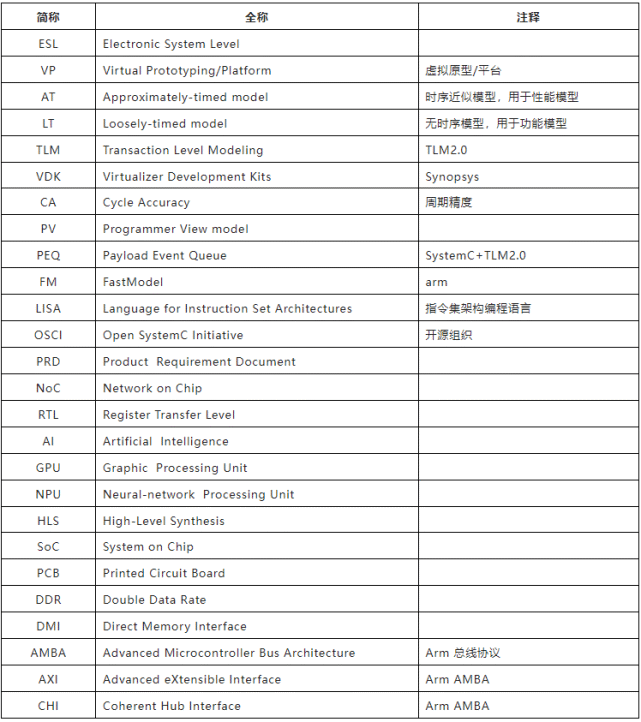
ESL发展及其在项目中的应用 原文链接:https://blog.csdn.net/xiaohaolaoda/article/details/131117987作者 | JJ.Tian, 复睿微电子ESL建模工程师一. 前言随着半导体行业的高速发展,ESL(Electronic System Level)建模或芯片建模在大算力高性能芯片领域显得越来越重要,国内外EDA或芯片设计公司都在构建自己的芯片评估工具或平台,以应对复杂芯片设计所带来的挑战。希望通过这篇文章让大家对ESL建模以及相关的基本概念和设计方法有一定的认识,了解ESL建模的方法和流程,理解工具并利用工具创造价值。本文主要介绍ESL相关的基础知识、概念、术语、以及ESL发展历史。基于这些新的理念和方法,ESL建模得到了长足发展并且逐渐趋于完善。与其它技术类似,ELS或芯片建模采用的工具平台也包括商业和开源两大阵营。此外,本文还介绍了芯片建模标准规范,IEEE1666-2011 SystemC+TLM2.0。在此基础上,还介绍了芯片建模的主要应用领域,有些应用比较成熟,比如性能模型(架构探索/评估/分析),功能模型(软件提前开发),功耗模型(功耗评估),混合仿真(功能或性能模型),软硬件协同设计,验证与划分等。有些应用比较新颖,比如高阶综合(HLS),主流的EDA供应商已经发布了相应的工具,由于应用领域局限性而尚未得到广泛应用。限于篇幅,本文只涉及性能模型和功能模型两个应用方向,其它方向的应用后续有机会再作介绍。在本文中,ESL、ESL建模、芯片建模,名称不同但是含义相当。二. 术语三. ESL发展简介早在20年前,随着芯片行业的发展,芯片结构越来越复杂,版本迭代越来越快速,应用场景越来越多样化,这些变化给芯片设计带来了巨大的挑战。人们注意到传统的设计方法已经不能再满足芯片设计需求,亟需一种全新的设计方法和理念,既能处理复杂的内部结构,又能应对功能的快速迭代,由此ESL应运而生。2001年,ESL率先由Gartner Dataquest定义和发布,并被大众所熟知,至今,ESL已经在芯片设计、验证以及仿真领域得到广泛应用。如果深入研究ESL的本质,它不是某种具体的设计语言、工具或平台,而是一种通用的设计和验证方法学,根据芯片各阶段的设计要求,在规格定义阶段(前期)、中期、后期利用这种方法对芯片的性能,功能,功耗进行建模,通过仿真得到某些参数或指标,作为芯片设计和优化参考。ESL主要应用领域:·性能/架构模型(CA/AT):架构探索,评估与优化,架构设计阶段·功能模型(TL):软件提前开发,软硬件并行开发,缩短研发周期·功耗模型:功耗评估·系统设计(System Level Design):软硬件协同设计、验证与划分·Co-simulation(Model+RTL)混合仿真:包括功能和性能仿真·高阶综合(HLS):使用工具将C++/SystemC+TLM2.0模型直接综合成RTL代码ESL之所以能应用于不同领域,是因为采用了高级编程语言,建模灵活,快速迭代,可以实现不同抽象层次(Abstraction Level)的模型。如果非要从学术层面来定义ESL,可以理解为“利用适当的抽象来增加对系统的理解,并以具有成本效益的方式提高成功实现功能的可能性”。这里面涉及系统、抽象、软硬协同设计和验证以及功能实现等。业界根据这些设计方法和思想,经过多年发展,已经形成了开源和商用两大阵营,以下是业界具有代表性的仿真工具与平台。·开源· SystemC+TLM2.0· QEMU· GEM5· ……·商用· FastModel, arm· VDK, Synopsys· Simics, Wind River/Intel· ……除了以上列出来的仿真工具和平台之外,当然还包括其它开源和商用仿真工具,不胜枚举,详情可以参考[15]。由于商用工具需要购买license,有些公司与其IP深度绑定,形成了完整的生态链,处于垄断地位,授权价格昂贵且授权方式完全由供应商主导,对国内芯片公司不是特别友好。因此国内大多数公司把目标都转向开源仿真工具,开源工具中使用比较广泛的是GEM5和QEMU,两者都提供了丰富的模型和完整的软件,但他们之间也存在差异。GEM5和QEMU都有完整的处理器,总线和外设功能模型,可以快速搭建用户需要的模型,另外,还提供相应的驱动软件和系统软件包,可以更快的实现系统boot功能,用户只需要关注软件开发工作,这些只是功能模型方向的应用。另外GEM5还提供了业界主流架构的处理器(core)模型,如x86/arm/risc-v等,总线(NoC)等架构模型,可以进行性能仿真和评估。在学术界也非常流行,使用GEM5进行计算机或芯片架构探索,性能评估等,基于GEM5仿真所发表的学术论文特别多。对于多数自研IP的公司来说,比如AI/GPU/NPU等,通常还是基于C++/SystemC+TLM2.0建模,根据自研芯片规格来实现自定义架构模型,也会借用GEM5里面现成的模型。顺便提一下,SystemC+TLM2.0之所以重要,是因为商用仿真平台多数都是参考或基于SystemC+TLM2.0开发。比如大家所熟知的Synopsys VDK仿真平台,就是在开源SystemC+TLM2.0基础上,增加和增强了很多新的功能,以图形界面方式呈现,专门为用户提供了二次开发的接口和方法,究其最低层技术还是基于SystemC+TLM2.0标准实现的,另外Candence Xcelium,一种综合逻辑仿真器,也支持SystemC+TLM2.0模型仿真,SystemC+TLM2.0是芯片建模和仿真的重要基础。四. IEEE1666-2011标准为了能够更全面地认识SystemC+TLM2.0, 我们可以从产生背景、编程语言、参考仿真器等多个方面来了解。根据前面介绍,早在2000年左右,人们就提出了抽象层次设计概念以应对复杂芯片设计挑战,但是当时并没有统一的实现语言和工具,比如LISA/LISA+早在90年代就被提出了,是最早架构建模语言之一,迄今为止,在arm的FastModel里面仍然可以见到其身影,除了FastModel之外业界很少直接使用LISA/LISA+语言建模。直到2004年SystemC诞生,架构建模语言逐渐趋于收敛和统一,2011年OSCI发了SystemC 2.3.0,目前最新版本为2.3.4,随后被纳入IEEE标准,并正式发布IEEE1666-2011标准版本。直到今天,还是由OSCI开发和维护,同时OSCI隶属于标准组织Accellera并成为该组织下面众多技术标准之一。首先,SystemC+TLM2.0是全面兼容C/C++的类库(classlibrary),支持C++11/14特征(Feature),所以可以理解为SystemC+TLM2.0是基于C/C++的建模语言(Modeling language),作为一门编程语言,它一直都在不断升级和发展,根据官方资料显示,主要朝着多线程(Multithreading)、功能安全(Functional Safety)、错误注入(Error Injection等方向进行发展和演变。其次,SystemC+TLM2.0还是一种开源参考仿真器,可以通过离散事件实现进程之间通信和同步,在这里,进程可以理解为模块里面具备独立功能的逻辑电路,使用进程旨在描述独立功能的逻辑电路的“并行性”,如果从这个角度来讲,SystemC+TLM2.0编程具有协同程序(Co-routines)的思想,因此在建模的时候,总是要考虑进程(逻辑电路)之间是顺序关系还是并行关系。通过几张图(均来自IEEE1666-2011)介绍SystemC+TLM2.0的主要内容和构成。图1展示了SystemC Language Architecture,最底层是标准C++编程语言,在此之上包括两大块核心内容Core Language 和 Data Type。核心语言部分主要包括module(sc_module), port(sc_port/sc_export), interface(sc_interface), channel(sc_channel),clock(sc_clock), 调度器(scheduler),进程(thread/SC_THREA/SC_METHOD),括号里面是相应的类名、函数或宏名。Data Type用于描述硬件中的数据位宽,逻辑状态(高电平,低电平,高阻态,不确定态),以及数据和状态之间的操作等。在两大核心的基础上还包括进程之间的控制和交互使用的接口(Interface)和通道(Channel),如signal、buffer、mutex、semaphore等。具备这些建模的基本要素之后就可以根据芯片规格(Specification)对其建模了。图1. SystemC Language Architecture (IEEE1666-2011)如果只用SystemC提供的组件来建模,开发者不仅需要关注模块内部结构和功能实现,还需要关注模块之间的通信功能实现。这对开发者来说,无疑是增加了开发负担,也不利于开发更高抽象层次的模型开发,因为SystemC里面模块之间通信以channel为主,比如signal/fifo,这种方式虽然可以描述更加精准的硬件行为(CA),但是仿真效率低,对于芯片架构探索或开发前期来说并不适用。为了解决不能开发任意抽象层次模型和仿真效率低两大问题,OSCI还推出了TLM(Transaction Level Modeling)。在OSCI官方文档中对SystemC+TLM2.0最常用的描述为SystemC with TLM2.0,SystemC/TLM2.0或SystemC+TLM2.0。SystemC+TLM2.0实际上包括两块独立功能的内容,建模时会同时使用。参考图2,SystemC又是TLM2.0的基础,包含TLM1.0和TLM2.0,两个版本在实现方式和细节上有所不同,TLM1.0使用相对较少,本文不做介绍。由于TLM2.0设计更具有通用性,获得了广泛应用,TLM2.0不仅提供blocking/non-block/Debug/DMI transport接口,还实现了通用数据类型(generic payload)和通用的相位(phase),由这两个通用模块构成基础协议(Base protocol)。接口和基础协议组成通用层(Interoperability layer),通用层除了极大地方便建模外,还让不同公司开发的模型可以集成到同一个系统中。除了通用层之外,TLM2.0还提供了utilities class,可以作为golden simple,包括socket/callback register/blocking/ non-blocking transport等。其中simple_initiator_socket/ simple_target_socket极为常用。这些接口效率高且使用方便,应用非常广泛,对于大多数建模场景而言,使用自带utilities class基本满足要求,当然如果有特殊需求,例如增加时序或时钟信息,或对新的通信协议进行建模,可以在通用层的基础上开发全新的socket,比如AMBA协议簇里面的AXI /CHI等。图2. TLM2.0 Class (IEEE1666-2011)根据前文对SystemC+TLM2.0的介绍,现在可以研究一下SystemC+TLM2.0建模抽象层次与具体应用之间的关系。图3展示了建模方式(Coding Styles)以及抽象层次,应用场景可分为四类,即软件开发、软件性能分析、架构性能分析、硬件验证。可以根据仿真需求选择相应的coding styles和TLM2.0通用层来实现,比如transport/ socket等。建模抽象层次应根据要求而定,精度和抽象层次更是需要权衡考虑(Trade-off),同时还需要兼顾仿真效率。总的来说,对精度要求更高,则对建模抽象层次要求也更低,其仿真效率就越低(仿真慢),反之亦然。除了SytemC+TLM2.0存在这个客观局限之外,其它EDA工具也类似,纵观芯片设计链路中的EDA工具中,没有任何一个EDA工具可以全部覆盖设计和验证功能,都会存在自身的优势和劣势。即便如此,也可以使用不完美的工具得出相对满意的结果,如何充分利用好SystemC+TLM2.0需要综合考虑模型精度和仿真效率。以模型对时钟或时序要求为例,每一种应用场景对时钟或时序要求差异很大,硬件验证则需要确保时钟周期完全一致,架构探索和软件性能分析则只需要时钟或时序近似,软件开发则完全不需要考虑时序信息,只要保证数据正确即可。图3. Use cases, coding styles, and mechanism(IEEE1666-2011)五. 性能模型图4是简化版本的芯片设计流程,忽略其它步骤和细节,对于前端和后端而言,EDA公司可以提供明确的测试与验证平台(工具),包括方法和流程。但是对于架构设计来说,如何验证,使用什么工具或平台呢?假如芯片架构师收到了来自市场或客户的产品需求文档(Product Requirement Document, PRD),需要根据产品需求文档量化芯片的参数和指标,即定义芯片规格,确定芯片里面某些子模块的具体参数和行为,比如L1/L2/L3 cache size,总线带宽,关键模块之间的时延,内存架构等,芯片研发初期,此时RTL还未开始开发,更是没有任何平台配合应用场景来验证参数的正确性和合理性,因此如何验证架构设计成为芯片挑战之一。特别是AI/GPU/NPU等类似专用的芯片,对架构验证平台的需求尤为突出。架构模型或性能模型成为验证架构设计的主要工具或平台,在规格定义阶段并可以开始设计架构模型,迭代,测试和优化,将结果反馈给芯片架构师,不断精细化芯片参数,架构或性能模型应当具备以下几点要求:模型精确性,抽象层次,可定量或定性分析模型迭代,参数可配置,可快速迭代,可探索全新的架构(下一代)图4. 芯片设计流程(简化)参考图4,芯片架构验证就是建模、测试、校验和优化的过程。尽管芯片架构验证处于芯片设计初期,实际上这一过程伴随芯片设计整个周期。架构探索可以分为单元架构(处理器微架构/存储架构)和系统架构,单元架构模型更聚焦于内部实现细节和交互信息,比如处理器5级流水,取指、解码、执行、访存、写回。而系统架构则侧重于整体性能评估,将应用场景实例化之后,直接加载到架构模型上运行,通过收集数据处理信息,比如Latency/Bandwidth/Efficiency/Event/Timing等等,定量分析架构的性能和参数。抽象层次其实是架构模型在建模之前需要考虑的重点。从周期精度模型(CA model),时间近似模型(AT model)到行为模型(LT/Behavior Model),需要根据评估目标而定,无关性能的模型,可以采用行为模型,需要关注性能的模型可以使用周期精度或时间近似模型,将这些不同抽象层次的模型集成到同一系统,还能得到混合(Hybrid)模型,该模型可以满足某些特殊场景的测试和验证需求。图5展示了建模与仿真流程,以及与架构设计之间的关系。无论是软件还是硬件设计,都有一种设计理念,称为可执行规格(Executable Specifications),对于芯片设计而言,其意是指架构设计、架构建模和架构验证过程。可以直接将架构规格说明转化为可执行程序,定量分析架构设计。图5. 建模和仿真流程架构建模包含的内容很多,流程虽然简单,但是整个建模和仿真过程,可以粗略也可以精细,灵活多变,结果呈现方式和分析方法也是多种多样。经过仿真除了可以得到带宽(Bandwidth)、时延(Latency/Delay)、波形(Waveform)等最基本的数据之外,还可以获得状态、事件统计等信息。架构设计和架构建模互为补充,伴随参数调整、仿真迭代、仿真优化和结果分析等过程,直到最终得到满足应用要求的参数和结果。图6. 简单的NoC参数和性能分析用例图6给出了一个简单的NoC性能分析用例,在NoC的上行和下行接口上增加监测(Monitor),收集数据传输过程的参数。假设总线协议是AXI,CPU发送的数据包来自某个应用场景。可以调整BL(Burst Length)长度、Burst Size、Burst Type等以适配不同的NoC配置,直到满足要求的结果。六. 功能模型我们知道任何产品都有窗口期,每家公司都希望自己的产品尽快上市(Time-to-Market),更快更多地抢占市场。为了最大化地缩短开发和生产周期,每个行业都在使用新进的工具来进行并行开发。芯片设计也不例外,如果简单地将芯片设计划分为硬件和软件两部分,传统的设计流程是先硬件后软件,以串行方式进行。因为软件开发依赖于硬件平台,为了实现硬件与软件并行开发,功能模型使软硬件并行开发成为可能。功能模型(Function model)也称为虚拟原型(Virtual Prototyping VP),虚拟平台(Virtual Platform VP),它们的本质都是一样,如果说非要有些区别,虚拟原型更倾向于片上系统(System on Chip, SoC),虚拟平台涉及更大的系统,除了包括SoC之外,还包括其它子模型如NoC,DDR,Peripherals等,在这里,可以理解为板级(Printed Circuit Board,PCB)虚拟系统。软件设计左移(Shift-left)在芯片设计领域越来越被重视,左移就是为了实现软硬件并行开发。参考图7,如果将芯片设计简单分为架构,前端和后端设计三个阶段,使用传统设计流程,软件需要在RTL开发快结束的时候,才能在FPGA/Emulator平台开始软件开发和调试,参考图7中Emulation starting point。如果采用功能模型或虚拟原型(VP),在时间上可以提前至少8~12个月,给软件团队足够的时间来开发和优化软件,利用功能模型,可以开发firmware/driver/API/boot flow/Linux/software stack等,如果功能模型增加了时序和追踪(Trace)功能,还可以运行应用程序,用来分析软件的性能。通过两种方式对比,在时间上有绝对的优势,因此获得了广泛应用,比如VDK、Simics、利用SystemC+TLM2.0开发的功能模型等。图7. 芯片研发周期示意图与性能模型相比,功能模型是程序员视角模型(Programmer View, PV),只要保证寄存器精度和数据传输正确即可,无需关注时序以及链路上数据的具体传输过程。如果有额外的需求,比如分析软件性能,可以在模型里面增加时序(Timing)、事件(Event)等信息,建模非常灵活,完全可以根据需求增加相应的特征(Feature)或功能。图8. 功能模型内部结构由于功能模型不需要考虑时序和传输过程等因素,与性能模型比起来,相对简单很多,参考图8,典型的功能模型用例主要包括输入/输出接口,数据队列,控制逻辑,回调函数,寄存器,状态信息,中断信号等等。针对无时序模型SystemC+TLM2.0专门提供了blocking和DMI接口,即b_transport和get_direct_mem_ptr,通过调用这两个接口函数可以直接返回结果,调用接口函数过程中不会被其它模块或进程打断。此外,SystemC+TLM2.0还提供了时间解耦(Temporal Decoupling),仿真时钟精度(Time Resolution),全局量子时间(GlobalQuantum)等特征,充分利用non-blocking/DMI接口和这些特征可以巨大地提升功能模型的仿真效率。七. 总结首先,本文介绍了ESL发展历史,以及商用和开源两大阵营中主流仿真工具和平台。其次,还介绍了SystemC+TLM2.0标准规范,最后介绍了两个主要应用场景:性能模型(架构模型)和功能模型(虚拟原型)。尽管可以使用SystemC+TLM2.0创建任意抽象层次的模型,但是也存在不足之处,目前SystemC+TLM2.0只支持单线程,正是这个原因导致复杂的或抽象层次较低的模型仿真很慢(仿真效率低),从官方渠道可以得知,SystemC+TLM2.0正在朝着多线程、功能安全、错误注入等方向发展和演变,以解决仿真效率问题和拓展更多的应用领域。参考资料[1]. IEEE Standard for Standard SystemC Language Reference Manual, IEEE Std 1666-2011[2]. TLM_2_0_presentation[3]. ESL DESIGN AND VERIFICATION 2006[4]. A SystemC Primer 2002[5]. systemc-from-the-ground-up-2-edition 2004[6]. System Design with SystemC 2002[7]. Enhanced Virtual Prototyping (Featuring RISC-V Case Studies) 2021[8]. Complete Symbolic Simulation of SystemCModels2016[9]. https://en.wikipedia.org/wiki/Virtual_prototyping[10].https://www.intel.com/content/www/us/en/developer/articles/tool/simics-simulator.html[11]. https://developer.arm.com/Tools%20and%20Software/Fast%20Models[12]. https://www.synopsys.com/verification/virtual-prototyping.html[13]. https://www.qemu.org/[14]. https://www.gem5.org/[15]. A Survey of Computer Architecture Simulation Techniques and Tools, 2019作者介绍JJ.Tian, 复睿微电子ESL建模工程师,华中科技大学工学硕士,在服务器芯片测试和验证、CPU/AI芯片建模等领域积累了丰富的工作经验。关于复睿微电子复睿微电子是世界500强企业复星集团出资设立的先进技术型企业。公司目标成为世界领先的智能出行时代的大算力方案提供商,致力于为汽车电子、人工智能、通用计算等领域提供以高性能芯片为基础的解决方案。目前主要从事汽车智能座舱、ADS/ADAS芯片研发,以领先的芯片设计能力和人工智能算法,通过底层技术赋能。复睿微电子是复星智能出⾏⽣态的通⽤⼤算⼒和⼈⼯智能⼤算⼒的基础平台。复睿微电子以提升客户体验为使命,在后摩尔定律时代持续通过先进封装、先进制程和解决⽅案提升算⼒,与合作伙伴共同⾯对汽⻋智能化的新时代
-
cadence upf低功耗流程的仿真验证 本文是记录项目过程中遇到的奇巧淫技,如有遗漏或者不足,请大家改正和补充,谢谢。随着深亚微米技术的普及与发展,leakage功耗在整个功耗中的比重越来越大,比如45nm下,已经占到了60%以上,所以低功耗解决方案应运而生。目前已经有一套标准的低功耗设计流程,流程有CPF(cadence主导)和UPF(synopsys主导)两种,但技术趋势是UPF会大一统,所以本篇将为那些仍旧使用ncverilog而不是vcs仿真工具的苦逼们提供一些参考。目前常用的降低低功耗的方法有四种:多电压域、时钟门控、电源关断和动态电压频率调整。其中的时钟门控对验证影响较小,大家应该都接触过,而剩下的三个对验证工作影响较大,需要用到各个EDA厂商的低功耗解决方案。闲话就说这么多,那么cadence如何使用upf来实现低功耗流程的仿真验证呢?第一步,先得有UPF文件,根据设计需求,使用TCL建立脚本,建立和管理独立电压源、确定隔离、建立电平漂移等,一般是设计或者后端人员书写,验证工程师当然也可以写,具体内容参考IEEE 1801。第二步,仿真case中添加电源上电过程,使用$supply_on函数给相应VDD上电。第三步,将UPF嵌入到仿真命令中,即:irun -lps_1801 sim.upf -lps_assign_ft_buf -lps_iso_verbose ...或者1 ncvlog ...2 ncelab -lps_1801 sim.upf -lps_assign_ft_buf -lps_iso_verbose ...3 ncsim ...相关options解释如下:①-lps_1801 filename: 指定符合IEEE 1801标准的UPF文件;②-lps_assign_ft_buf: 指定assign赋值被当做buffer对待,而非默认的wire,好处是从always-on domain进入和穿过power-down domain的信号被force成x,便于debug;③-lps_const_aon: 对处在power-down domain并且直接和always-on domain相连接的tie-high或者tie-low constant,不使能corruption功能;默认不使用该功能;④-lps_enum_rand_corrupt:对于用户定义的enum类型数据,在电源关断后,随机从枚举列表中选择一个值作为变量值;和该命令相类似的还有-lps_enum_right, -lps_implicit_pso等,因为不常用,就不一一介绍了;⑤-lps_iso_verbose: 使能isolation的log功能,这个一般需要加上;⑥...其它的options请参考cadence的low-power simulation guide。最后,运行仿真即可。最后说一下low power流程验证正确性和完备性的确认方法。①增加的low power流程不能影响芯片本身功能的正确性,比如通过电源关断来降低芯片功耗,则关断再打开后,芯片还可以正常work。这部分可以利用原有的self-check验证环境来确认。②利用log文件分析,上述仿真命令-lps_verbose和UPF文件会为仿真输出与low power相关的warning, error以及assertion信息,通过log文件可以check流程的正确性;③自动的assertion checker分析,使用-lps_verify选项可以自动检查电源关断顺序(隔离->复位->断电)和电源打开过程(上电->解复位->解隔离),如不满足该时序要求,会自动报错;④利用覆盖率保证验证完备性,使用-lps_vplan选项依据UPF文件生成low power验证计划,通过simvision提供的coverage接口,得到low power相关的功能覆盖率;https://www.cnblogs.com/jyaray/p/4817777.html