
搜索到
344
篇与
的结果
-
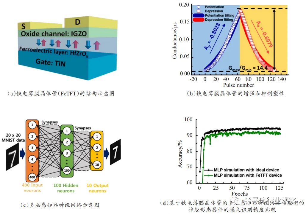
 神经形态晶体管研究进展 光刻人的世界2020年12月28日18:45神经元是大脑信息处理的基本单元,突触则是神经元之间在功能上发生联系的部位,也是信息传递和处理的关键部位。从底层出发研制具有生物突触和神经元功能的固态器件与系统对于研制超低功耗“类脑芯片”和实现全新一代人工智能系统意义十分重大。其中多端口晶体管由于其独特的电容耦合机制,多元化的界面调控手段和丰富的材料选择等优点,最近引起了科研界的广泛关注。从铁电突触晶体管、双电层/电化学突触晶体管、光电突触晶体管3类器件介绍近年来神经形态晶体管的研究进展,并总结该类器件面临的机遇和挑战。引言人脑是一个大规模并行计算结构,通过突触传递输入信息,能够实时处理接收到的各类信息,每个突触事件仅消耗1~10fJ,其高效和超低功耗一直为全人类所惊叹。大脑由大约1011个神经元组成,每个神经元可以通过1000多个突触与其他神经元连接。这些神经元和突触连接排列在三维空间中,形成了一个复杂的信息处理神经网络,它是人类所有感知、思想和行为的基础。在当今社会,人类已经步入了大数据时代,每天都要进行大量的数据传输和储存,这些工作如今主要都依赖于传统的计算机处理系统,其功不可没,然而传统计算机也面临着许多 的挑战。(1)构筑传统计算机的主要器件CMOS晶体管发展到当前工艺已经很难遵循摩尔定律了,传统计算机很难实现更小尺寸的高效处理模式;(2)传统计算机的构架遵循冯·诺依曼结构,其结构中CPU和内存是分开的。两者之间的大量数据传输不利于计算系统的效率提升,功耗降低,体积减小,即达到了“冯·诺依曼瓶颈”[1]。众所周知,相对于传统计算机,人脑能够快速处理复杂信息,同时学习和记忆,并且能耗非常低,体积很小,其高效和强大引起了众多科学家的关注[2-3]。受大脑这样的生物超级计算机的强大能力鼓舞,利用电子器件构筑一个能够自学习低功耗类脑计算机的神经形态工程理念于几十年前就已经提出来了。发展至今,科学家们提出类脑神经计算可由两类途径实现,分别是软件模拟和硬件实现。目前基于软件模拟的方法往往需要消耗大量的能量和占据很大的空间。IBM曾用超级计算机(Blue Gene)来进行软件模拟,其电功耗高达1.4兆瓦[4]。此外,软件模拟的途径是通过计算机大量串行处理进行计算,因此不能高效地模拟神经网络的并行处理机制。基于硬件实现的途径是利用高集成度的电子器件来构建人工神经元网络。突触作为神经元的功能连接部位,能够高效地处理和传递信息,也是计算和学习的基本单位。因此,设计并制备出具有突触功能的电子器件装置对于实现类脑计算体系存在着非凡的意义。神经系统中,突触作为一种特殊的结构,它能够将电信号转化为化学信号,再转化为电信号,从而进行神经元之间的信息传递。根据后神经元响应的电信号不同可分为兴奋性突触电流/后电位(excitatory post-synaptic current/potential, EPSC/EPSP)和抑制性突触后电流/后电位(inhibitory postsynaptic current/potential,IPSC/IPSP)。前神经元和后神经元之间的连接强度被定义为突触权重,许多突触权重变化的研究统称为突触可塑性。根据保留时间的不同,突触可塑性可以简单地分为短程可塑性(short-term plasticity,STP)和长程可塑性(long-term plasticity, LTP)。STP发生在毫秒到分钟之间,是神经网络计算功能的生理基础。双脉冲易化(pairedpulse facilitation,PPF)是STP的一种表现形式,当第二个输入信号跟第一个输入信号时,突触后信号被放大。PPF可参与一些神经元任务,如简单的学习和信息处理。LTP表示持续几个小时或更长时间的可塑性变化,将给神经网络带来永久性的变化,从而使大脑能够存储大量的信息。Hebb假设认为持续和反复刺激突触前神经元,可导致突触后神经元突触传递效率的提高[5]。时间依赖突触可塑性(spiketiming-dependent plasticity,STDP)概念的提出进一步完善了Hebb的理论,指出突触前和突触后尖峰的时间关系可以调节突触权重[6]。除STDP外,频率依赖突触可塑性(spike-rate-dependent plasticity,SRDP)是另一个基本的学习机制,突触权重可以通过控制突触前脉冲频率来改变,高于特定频率阈值的高频突触前脉冲将引起突触后反应增强,而低于特定频率阈值的低频突触前脉冲会导致这种反应的抑制[7]。近年来,大量的电子器件被构筑出来模拟突触塑性以期其在类脑神经形态工程中的突破和应用。其中两端器件如忆阻器、相变存储器、原子开关等,由于它们具有结构简单、功耗低、物理体积小、易于大规模集成等优点已被广泛应用于模仿突触功能[8-9]。然而,这些器件很难同时执行信号传输和自学习功能,大大阻碍它们在先进类脑神经形态工程中的进一步应用[10]。三端/多端突触晶体管不仅克服了二端器件很难同时执行信号传输和自学习的缺点,还具有稳定性好、测试参数相对可控、运行机制清晰、可由多种材料构成等优点[11]。通过适当的材料选择和结构设计,三端/多端突触晶体管可以将外界的刺激(光、压力、温度等)转换成电信号,从而实现对外界环境直接响应的人工突触[12-13]。此外,模拟需要多端操作的并行学习和树突整合可以很容易地在基于三端/多端突触晶体管的人工突触中实现,这为开发具有较少神经元件的神经网络开辟了可能 性。因此,三端/多端突触晶体管可能比其他类型的器件更适合模拟突触功能。基于三端/多端突触晶体管的人工突触的研究越来越受到重视,但这一领域还处于起步阶段。本文综述和讨论了包括铁电突触晶体管、双电层/电化学突触晶体管和光电突触晶体管在内的三端/多端晶体管的工作原理和近年来的主要进展,以期对今后的研究有所启发。铁电突触晶体管铁电场效应晶体管(ferroelectric field-effect transistors,FeFETs)具有编程速度快、无损读出、开关比大、低功耗等优点,在人造电子突触仿生学方面有广泛的应用前景[14]。FeFETs应用于突触晶体管的工作原理是由于具有高介电常数能够自发极化的铁电材料作为其绝缘层,通过电压可以调控铁电材料的极 化状态,从而改变沟道载流子密度,而沟道电导非易失性改变实现了突触功能的模拟。此外,每一个脉冲电压都会改变铁电材料的细微极化状态,因此也会在沟道中得到不同的电导。利用这种多级化非易失性的变化可用于记录突触权重,许多科学家利用这一性质模拟了突触的STDP学习功能。2014年,Kaneko等[15]提出基于ZnO/Pr(Zr,Ti)O3/SrRuO3/Pt结构的铁电晶体管构筑神经网络。利用铁电材料Pr(Zr,Ti)O3(PZT)的多极化效应可调控晶体 管中沟道ZnO中电导的大小,这种调节变化可保持很长的时间,类似长程可塑性。使用此铁电晶体管成功地模拟了生物突触中的STDP学习规则,此外为了实现模式识别功能利用此器件搭建了神经网络结构,其原理是由于STDP学习规则进行了学习和记忆,其网络结构中的权值分布会发生改变,进行识别操作过程时,当输入一定模式时,神经网络会召回最接近曾经学习过的模式形成输出信号。虽然基于PZT的铁电晶体管在模拟突触方面表现出很好的塑性行为,但其固有的铅含量,不可避免地会给人类和环境带来危害。近年,Kim等[16]报道了一种如图1(a)所示以24nm HfZrOx为铁电绝缘层10nm InGaZnO为沟道层的突触晶体管。HfZrOx首先由ALD在280℃的腔体温度下沉积,然后在400℃氮气 氛围下退火1min形成铁电绝缘层。通过改变施加的电压脉冲的振幅,可以精细地调制通道的电导。此外,如图(1b)所示构筑的铁电晶体管表现出很好的增强和抑制塑性,例如高的模拟状态数(64)、良好的线性(Ap,-0.8028;Ad,-0.6979)和Gmax/Gmin比值>10。受其良好性能的鼓舞,设计了一个如图1(c)所示具有400个输入神经元、100个隐藏神经元和10个输出神经元的多层感知器神经网络。经过多阶段训练,实现了手写数字91.1%的识别准确度,接近理想突触神经网络94.1%的识别率,如图1(d)所示。氧化物铁电材料通常需要较高的结晶温度,这限制了其在塑料基板上大面积电子器件的应用。此外,其固有刚性也限制了其在柔性和可穿戴电子设备领域的应用。图1.无机铁电晶体管的神经形态应用与氧化物铁电体相比,有机铁电体可以克服氧化物铁电体的这方面的局限性。Jang等[17]报道了以有机PVDF-TrFE薄膜作为铁电绝缘层的超薄(500nm) 突触晶体管,如图(2a)所示。它可以独立存在,无需基底或封装层,利用简单的干法剥离和粘贴方法,所制备的器件可以稳定地转移到如图2(b)所示的二氧化硅、纺织品、牙刷、果冻、糖果等各种均匀和不均匀的基板上。通过对有机铁电绝缘层的极化调节,成功地实现了短程可塑性(STP),长程可塑性(LTP),长程抑制(LTD),时间依赖突触可塑性(STDP)等重要的突触功能,如图2(c)~(e)。为了验证超薄有机突触晶体管能在苛刻的弯曲条件下保持其稳定的突触功能,他们在R=50µm,ε=0.48%的折叠条件下测试了器件突触的突触塑性,图2(f)展现了苛刻的弯曲条件下施加6000个脉冲器件表现 出稳定的长期增强和长期抑制突触塑性。这项工作表明了超薄柔性有机人工铁电突触器件是实现未来可穿戴智能电子的关键技术之一。图2.超薄柔性有机铁电晶体管的突触塑性双电层/电化学突触晶体管双电层/电化学突触晶体管(electric-double-layer/electrochemical synaptic transistors)由于其栅介质层中离子可以自由移动,在电场诱导作用下进行迁移、积聚进而改变沟道导电特性。晶体管中的栅电极可以看作是突触前膜,沟道层可以看作是突触后膜,沟道电导可以看作是突触重量,这种类似于突触的工作模式使其在低功耗,柔性突触仿生学领域展现了广泛的应用前景。在外电场作用下界面处由于静电耦合积累电荷层的晶体管称为双电层薄膜晶体管[18],而对于有些离子可渗透的半导体,当施加的外电场过大,离子可从栅介质层中渗透进沟道层中进而改变沟道电导的工作原理是电化学掺杂,其晶体管称之为电化学薄膜晶体管[19]。突触电子学中常用易失性的静电耦合作用和非易失性的电化学掺杂/脱掺杂这两种机制来模拟突触的短程和长程可塑性。此外,双电层/电化学突触晶体管一个出众的方面是在低功耗方面已经能够实现生物学中单个突触事件的能量消耗(大约10fJ/spike)[20],这为实现超低功耗突触器件打下了坚实的基础。无机半导体具有良好的稳定性和较高的载流子迁移率,在三端双电层/电化学突触晶体管中彰显着巨大的应用潜力。近年来用于突触器件的无机半导体材料有很多,包括碳纳米管[20],石墨烯[21],二硫化钼[22],铟锌氧[11],铟镓锌氧[23]等。碳纳米管具有纳米尺寸和独特的电学性质,被认为是未来电子电路中 替代硅的潜在材料。2013年,Kim等[20]报道了以碳纳米管作为沟道层,氢掺杂聚乙二醇单甲醚(PEG)作为栅介质层的突触晶体管,其结构示意图如图3 (a)所示。在施加电压脉冲之前,聚合物中的氢离子是随机分布的。当正电压脉冲作用于碳纳米管突触器件的栅极时,氢离子开始定向移动,最终由于静电 耦合效应形成双电层,进而调节碳纳米管沟道中载流子浓度,导致沟道电流的增加。脉冲结束后,由于浓度梯度的存在,电解质/沟道界面附近的氢离子会从界面处开始慢慢扩散,使沟道电流继续减小直至稳定,如图3(b)。基于离子迁移和非易失性静电耦合效应,该晶体管成功地模拟了EPSC、PPF、动态逻 辑、长程增强塑性、长程抑制塑性和STDP等典型的突触功能。图3.碳纳米管突触晶体管示意图及突触前电压脉冲触发的EPSC石墨烯具有优异的热稳定性、超薄的层状结构和良好的力学性能,是一种应用于高集成度柔性电子器件领域的理想材料。Sharbati等[21]利用聚氧化乙烯(PEO)中的LiClO4作为固体电解质,被剥落下来的石墨烯原子层作为沟道层。栅电极模拟突触前膜,固体电解质模拟神经元间传导离子的突触裂缝。通过控制石墨烯层中锂离子的浓度,实现了对石墨烯器件电导的可逆精确调节。在这个电化学石墨烯突触器件中模拟了突触的增强和抑制塑性。当向石墨烯器件施加50pA、10ms的输入电流时,沟道电阻立即下降30Ω,然后衰减到稳定状态,此时的电阻比初始状态小10Ω,这种现象模拟了兴奋性突触的突触权重变化,电导的永久性变化是锂掺杂的非易失性造成的。在应用一系列不同参数的脉冲后,还观察到LTP和LTD行为。STDP塑性也在这种电化学突触中通过应用双脉冲可编程方案得到了证实。种种突触行为的成功模拟预示着这种电化学石墨烯突触晶体管有可能成为神经形态计算的硬件实现方案之一。近年来,原子层状的2D材料已经引起了纳米器件的广泛关注,在各类先进的电子器件方面表现出很好的应用前景。Jiang等[22]制备了一种以聚乙烯醇(PVA)质子传导电解质为栅介质层的多栅调控2D MoS2突触晶体管。共面金属电极2DMoS2分别被认为是突触前膜和突触后膜。通过调控多个突触前输入端可以在这样的2D MoS2神经形态晶体管中进行时空耦合。基于2D MoS2的器件中已经成功模拟了EPSC、PPF、动态滤波器、时空信号树状积分等突触行为。此外,乘法神经编码和神经元增益调制也被成功证明。这种2D MoS2神经形态装置对于在二维纳米级神经形态认知系统中实现有趣的人工智能具有重要意义,如方向选择性、目标识别、感知处理等。金属氧化物半导体由于其高的载流子迁移率、优异的光学透明性、良好的稳定性以及可大面积制备等优点使其成为人工突触晶体管的潜在候选沟道材料。其中铟锌氧(IZO)和铟镓锌氧(IGZO)是应用最广泛的氧化物材料。Zhu等[11]提出了一种基于磷(P)掺杂纳米颗粒SiO2薄膜质子横向耦合效应的IZO突触晶体管。如图4(a)所示,不需要底部导电,并且栅极电压可以仅通过一个横向双电(EDL)电容直接耦合到IZO半导体实现横向调控。使用该器件模拟了一系列短程可塑性行为,包括两个脉冲时间间隔Δtpre越小可获得较高的PPF数值的双脉冲易化(如图(4b)所示),高频信号越多,突触权重在短时间内增加越多的高通滤波行为(如图4(c)所示)以及时空相关动态逻辑测试(如图4(d))。此外,这种横向耦合的突触晶体管可以很容易扩展到多个输入栅极,以构建突触相互作用的功能。这里提出的这种基于质子传导电解质的横向耦合IZO晶体管对突触电子学和神经形态工程具有重要意义。图4.横向耦合IZO晶体管的突触塑性2019年,He等[23]展示了一种基于金属氧化物铟镓锌氧(IGZO)多端口神经晶体管,模拟了不同时空输入模式的树突辨别,其结构示意图如图5(a)所 示。首先,该器件模拟了突触可塑性的调节行为,如双脉冲易化和高通时间滤波。然后在多端神经晶体管中实现了不同时空输入模式的树突识别,说明它可以作为基本皮层计算的时空信息处理单元,大大减小神经形态系统的规模和复杂性,提高人工神经网络的效率。最后,作为一个时空信息处理的例子,一个有趣的工作——通过基于这种多端IGZO神经晶体管的人工神经网络来模拟人脑的声音定位功能被提出来,利用双耳效应在人脑中定位声音的示意图如图5(b)所示。如图5(c)所示,当声音来自右侧方向时,POSTN1首先处理弱突触传递的信号,然后处理强突触传递的信号。POSTN2首先处理强突触传递的信号,然后处理弱突触传递的信号。因此,在最后一个PREN信号出现时,POSTN1(IPOST1)的突触后电流幅度大于POSTN2(IPOST2)。同样,如果声音是从左方发出的,则IPOST2的振幅大于IPOST1的振幅。最后一个PREN信号时,IPOST和IPOST1的振幅与PREN 2和PREN1峰值(TPREN2-TPREN1)的相对时间和声音方位角的比值如图(5d)所示。最后一个PREN信号时,IPOST1和IPOST2之间的差变随着PREN 1和PREN 2峰值相对时间的变化。当时差为0ms时,比率为1。当时间差在25~1000ms变化时,比值大于1,并且随着时间差的增大而增大。当时间差在-1000~-25ms之间变化时,比值小于1,并且随着时间差的增大而增大。这种与时间相关的识别表明了人工神经网络对声音方位角的检测功能。图5.多端双电层晶体管神经形态模拟有机半导体由于其成本低,化学多功能性强,柔性可弯曲,易于加工等优点被国内外各大实验室所研究,其也被用来制备有机电化学晶体管来模拟突触塑性。2015年,Gkoupidenis等[24]首次报道了使用PEDOT:PSS作为沟道层,KCl 电解质作为栅绝缘层的低功耗有机电化学神经形态晶体管。电解液中的离子由于电场作用会被注入到PEDOT:PSS聚合物中以改变其空穴掺杂水平,从而调节流经通道的空穴电流。当脉冲电压被移除时,由于先前注入的离子会扩散回电解质,PEDOT:PSS将恢复到原来的状态。基于PEDOT:PSS的电化学突触晶体管实现了双脉冲抑制(PPD)和动态滤波特性等典型的突触行为。近年来,Qian等[25]将聚(3-己基噻吩)(P3HT)旋涂在SiO2/Si衬底上作为沟道层,热沉积了金作为源、漏和栅电极,最后将配比的离子凝胶作为栅绝缘层制备了有机电化学晶体管,其结构如图6(a)所示。利用施加在栅极的脉冲电压作为输入刺激,沟道电导变化代表突出权重。该突触晶体管成功模拟了后突触兴奋电流(如图(6b)所示),当施加脉冲栅电压,阴离子从离子凝胶移动到栅绝缘层与沟道层的界面处,从而形成EDL。因此,P3HT中的空穴积聚在半导体和离子凝胶的界面上,导致通道电导增加。在脉冲电压撤去后,阴离子开始扩散,回到它们在离子凝胶中的初始分布,因此PSC恢复到原来的状态。基于P3HT的有机电化学晶体管也实现了自我调整(如图6(c)所示)。当一系列的输入脉冲电压施加时,双脉冲易化出现在前两个尖峰上,但随后EPSC值随着脉冲电压的持续增加而减少,这种现象与生物兴奋性突触的适应性相同。此外,如图6(d)所示该突触晶体管还实现了双栅调控的OR逻辑。图6.有机电化学晶体管的突触塑性模拟光电突触晶体管光电突触晶体管(optoelectronic synaptic transistors)是构成神经形态计算系统的另一基本方法,利用这种新型人工装置模拟突触行为具有高效节能的优势。相对于传统的突触装置需要额外的传感器来进行光电转换。而以光为输入信号的光电神经形态器件,不仅将视觉、信息处理和记忆结合在一起,而且具有带宽高、鲁棒性强、并行性好等优点,适用于模拟人眼视网膜神经元等功能[26-27]。2018年,Yang等[28]制造了基于铟镓锌氧(IGZO)双电层(EDL)晶体管的电阻负载反相器用于光电突触器件应用。这种光电人工突触装置可以模拟突触 行为,如兴奋性突触后电位(EPSP),双脉冲易化(PPF)和长期可塑性等。整个器件可以看作是一种低压光电人工突触。其施加在IGZO通道层上的光脉冲 ,输出电位和沟道的电导改变分别被视为输入信号,突触后电位(PSP)和突触权重,其结构示意图如图7(a)所示。图7(b)的上部和下部分别描绘了不同光脉冲功率(232mw/cm²在和176mw/cm²)在不同栅压下刺激的EPSP曲线。从图中观察到更强的光脉冲信号导致更显著的反应,输出端电位从基态急 剧升高,达到峰值后,突触后电位逐渐回落。在这个过程中,通道电阻被输入光脉冲调制,导致输出电压相应地改变。图7(c)显示了两个连续的突触前光脉 冲触发的EPSP(PPF塑性行为),由第二个突触前光脉冲触发的EPSP的振幅比由第一个突触前光脉冲刺激的EPSP的振幅大1.37倍。图7(d)描述了不同 栅压下,刺激次数累积时,器件突触权重变化情况。图7.基于铟镓锌氧(IGZO)双电层(EDL)晶体管的光电突触塑性同年,Dai等[29]报道了一种有机场效应晶体管的光电突触装置,该装置使用聚丙烯腈(PAN)膜作为介电和电荷捕获层,PAN介质薄膜的强极性官能团可以在沟道/栅介质的界面上产生很强的电荷俘获效应。界面处光生电荷的捕获和去捕获过程为OFET提供了突触行为,如EPSC和PPF。此外,通过调节光刺激参数(包括光脉冲宽度、强度和光脉冲数量),实现了类似于人脑的记忆和学习行为。包括EPSC衰退和遗忘等行为。Wang等[30]报道了一种无机卤化物钙钛矿(CsPbBr3)量子点(QD)的光子突触。将厚度为30nm的CsPbBr3QD层旋涂到100nm厚的SiO2的Si衬底上。超薄的聚甲基丙烯酸甲酯(PMMA)层被旋涂在顶部作为钝化层。然后在PMMA顶部沉积p型并五苯作为半导体沟道。最后通过热蒸发和掩膜版技术沉积金的源、漏电极,该器件结构如图8(a)所示。器件中CsPbBr3量子点和半导体层之间形成的异质结构是该器件的光学可编程和电可擦除特性的基础。在栅极作用下,CsPbBr3量子点中的光生空穴通过能带调控下很容易注入到半导体层,而电子则留在CsPbBr3量子点中。而由于势阱的存在,留在CsPbBr3量子点中电子能保持较长时间从而产生类似突触的记忆效应。想要完全擦除这种记忆效应则需要加一个足够的负栅极电压。利用这种特性,通过光脉冲宽度、光脉冲强度和光脉冲波长等光刺激参数,有效地模拟了EPSC、PPF、PPD等突触塑性,如图(8b)~(d)所示。此报道中光电突触装置的制备有望为今后神经形态器件的设计提供新的思路。图8.有机场效应晶体管的光电突触塑性总结和展望近10年来,在神经形态工程的飞速发展进程中,基于硬件途径实现人造突触得到了充分的重视和研究,从模拟生物突触或神经元行为,到复杂的神经形 态计算 ,都取得了显著的进展。其中三端口晶体管由于具有稳定性好、测试参数相对可控、运行机制清晰、可由多种材料构成等优点在众多被构筑出来用以模拟突触行为的电子器件中脱颖而出。通过适当的材料选择和结构设计,三端/多端突触晶体管可以将外界的刺激(光、压力、温度等)转换成电信号,从而实现对外界环境直接响应的人工突触。此外,三端/多端突触晶体管还具有同时执行信号传输和自学习的优势,而且模拟需要多端操作的并行学习和树突整合可以很容易地在基于三端/多端突触晶体管的人工突触中实现,这为开发具有较少神经元件 的神经网络开辟了可能性。本文讨论了包括铁电突触晶体管、双电层/电化学突触晶体管和光电突触晶体管在内的三端/多端晶体管近年来的最新进展。它们有各自的优缺点,其中铁电场效应晶体管具有编程速度快、无损读出、开关比大、低功耗等优点。然而部分改变铁电材料的极化状态通常需要较大的工作电压,铁电材料的稳定极化状态使其易于实现LTP,但是很难实现STP;双电层/电化学突触晶体管在实现逻辑功能、树突整合和人工树突神经元方面优于其他类型的器件。此外,双电层/电化学晶体管的低压工作特性也为实现超低能耗的突触器件提供了可能。然而,器件的耐用性和电解质的不稳定性可能是双电层/电化学突触晶体管的主要限制;在光电突触晶体管方面,以光为输入信号的光电神经形态器件,不仅将视觉、信息处理和记忆结合在一起,而且具有带宽高、鲁棒性强、并行性好等优点,适用于模拟人眼视网膜神经元等功能。然而,利用光信号实现抑制性突触仍然是一个很大的挑战。这些器件各有优缺点,根据特定应用程序的要求,一种类型的器件可以优先于其他类型的器件。神经形态工程旨在构建具有超低能耗的鲁棒类脑计算机,利用新兴的突触装置来实现人工神经网络已经有了很多成功的尝试,然而神经形态器件领域所面临的一些主要问题和挑战仍需要我们不断进取努力。例如:目前所报道的突触器件模拟的小部分突触行为,完整的人造突触功能还需进一步研究完善;对于能够模拟生物神经元信息处理功能的神经形态器件的研究还仅限于少数报道,迫切需要更 深入的研究;目前科学对人脑的功能和运行机制的了解还在初步阶段。虽然目前这一领域还处于起步阶段,但是在未来,期待利用大量人造突触晶体管模拟类似于感官(视觉、听觉、运动、嗅觉)这样复杂的人类神经系统。相信通过物理、化学、材料学、计算机和医学等科学领域的跨学科交流,类脑神经形态工程将获得不断的革新进步和应用,先进的人工智能系统将促进人类在服务行业、个人医疗、教育和交通等领域的生活。文献引用:朱力,万青. 神经形态晶体管研究进展[J]. 微纳电子与智能制造, 2019, 1(4): 39-50.Research progress of neuromorphic transistors[J]. Micro/nano Electronics and Intelligent Manufacturing, 2019, 1(4): 39-50.《微纳电子与智能制造》刊号:CN10-1594/TN主管单位:北京电子控股有限责任公司主办单位:北京市电子科技科技情报研究所北京方略信息科技有限公司投稿邮箱:tougao@mneim.org.cn(网站:www.mneim.org.cn)参考文献:[1] BACKUS J. Can programming be liberated from the von Neumann style? a function style and its algebra of programs[J]. Communications of the ACM, 1978, 21(8): 613-641. [2] DRACHMAN D A. Do wo have brain to spare[J]. Neurology, 2005, 64 (12):2004-2005. [3] FURBER S. To build a brain[J]. Spectrum IEEE, 2012, 49(8): 44-49. [4]MARKRAM H. The blue brain project[J]. Nature Reviews Neuroscience, 2006, 7(2): 153-160.[5] MARKRAM H, GERSTNER W, SJÖSTRÖM P J. A history of spike-timing-dependent plasticity[J]. Frontiers in Synaptic Neuroscience, 2011, 3(4): 4. [6] CAPORALE N, DAN Y. Spike timing-dependent plasticity: a hebbian learning rule[J]. Annual Review of Neuroscience, 2008, 31(1): 25-46. [7] RACHMUTH G, SHOUVAL H Z, BEAR M F, et al. A biophysically- based neuromorphic model of spike rate- and timing-dependent plasticity[J]. Proceedings of the National Academy of Sciences, 2011, 108(49): E1266-74. [8] PREZIOSO M, MERRIKH-BAYAT F, HOSKINS B D, et al. Training and operaion of an integrated neuromorphic network based on metal- oxide memeristors[J]. Nature, 2015, 521(7550): 61-64. [9 ] XU W, LEE Y, MIN S Y, et al. Simple, inexpensive, and rapid approch to fabricate cross- shaped memristors using an inorganic- nanowire- alignment technique and a one- step reduction process[J]. Advanced Materials, 2016, 28(3): 527-532. [10] NISHITANI Y, KANEKO Y, UEDA M, et al. Three-terminal ferroelectric synapse device with concurrent learning function for artficial neural networks[J]. Journal of Applied Physics, 2012, 111(12): 124108-1-124108-6. [11] ZHU L Q, WAN C J, GUO L Q, et al. Artificial synapse network on inorganic proton conductor for neuromorphic systems[J]. Nature Communications, 2014, 5: 3158. [12] DAI S, WU X, LIU D, et al. Light- stimulated synaptic devices utilizing interfacial effect of organic field-effect transistors[J]. ACS Applied Materials & Interfaces, 2018, 10 (25): 21472-21480. [13] WANG K, DAI S, ZHAO Y, et al. Light-stimulated synaptic transistors fabricated by a facile solution process based on inorganic perovskite quantum dots and organic semiconductors[J]. Small, 2019, 15(11): 1900010-1-19000010-8. [14] MILLER S L, MCWHORTER P J. Physics of the ferroelectric nonvolatile memory field effect transistor[J]. Journal of Applied Physics, 1992, 72(12): 5999-6010. [15] KANEKO Y, NISHITANI Y, UEDA M. Ferroelectric artificial synapases for recognition of a multishaded image [J]. IEEE Transactions on Electron Devices, 2014, 61 (8): 2827-2833. [16] KIM M K, LEE J S. Ferroelectric analog synaptic transistors[J]. Nano Letters, 2019, 19(3): 2044-2050. [17] JANG S, JANG S, LEE E -H, et al. Ultrathin comformable organic artificial synapses for wearable intelligent device applicatios[J]. ACS Applied Materials & Interfaces, 2019, 11(1): 1071-1080. [18] MIN Y, AKBULULUT M, SANGORO J R, et al. Measurement of forces across room temperature ionic liquids between mica surfaces[J]. The Journal of Physical Chemistry C, 2009, 113(37): 16445-16449. [19] KIM S H, HONG K, XIE W, et al. Electrolyte-gated transistors for organic and printed electronics[J]. Advanced Materials, 2013, 25(13): 1822-1846. [20] KIM K, CHEN C L, TRUONG Q, et al. A carbon nanotube synapse with dynamic logic and learning[J]. Advanced Materials, 2013, 25(12): 1693-1698. [21] SHARBATI M T, DU Y, TORRES J, et al. Low- power, electrochemically tunable graphene synapses for neuromorphic computing[J]. Advanced Materials, 2018, 30 (36): 1802353. [22] JIANG J, GUO J, WAN X, et al. 2D MoS2 neuromorphic devices for brain- like computational systems[J]. Small, 2017, 13(29): 1900933-1-1700933-11. [23] HE Y L, NIE S, LIU R, et al. Spatiotemporal information processing emulated by multiterminal neuro- transistor networks[J]. Advanced Materials, 2019, 31(21): 1900903-1-19000903-8. [24] GKOUPIDENIS P, SCHAEFER N, GARLAN B, et al. Neuromorphic functions in PEDOT: PSS organic electrochemical transistors[J]. Advanced Materials, 2015, 27 (44): 7176-7180. [25] QIAN C, SUN J, KONG L A, et al. Artificial synapses based on in- plane gate organic electrochemical transistors[J]. ACS Applied Materials & Interfaces, 2016, 8 (39): 26169-26175. [26] KURAMOCHI E, NOZAKI K, SHINYA A, et al. Largescale integration of wavelength- addressable all- optical memories on a photonic crystal chip[J]. Nature Photonics, 2014, 8(6): 474-481. [27] GHOLIPOUR B, BASTOCK P, CRAIG C, et al. Amorphous metal- sulphide microfibers enable photonic synapses for brain-like computing[J]. Advanced Optical Materials, 2015, 3(5): 635-641. [28] LI H K, CHEN T P, LIU P, et al. A light-stimulated synaptic transistor with synaptic plasticity and memory functions based on InGaZnOx- Al2O3 thin film structure [J]. Journal of Applied Physics, 2016, 119(24): 244505- 1-244505-5. [29] DAI S L,WU X H, LIU D P, et al. Light-stimulated synaptic devices utilizing interfacial effect of organic fieldeffect transistors[J]. Applied Materials & Interfaces, 2018, 10(25): 21472-21480. [30] WANG Y, LV Z Y, CHEN J R, et al. Photonic synapses based on inorganic perovskite quantum dots for neuromorphic computing[J]. Advanced Materials, 2018, 30 (38): 1802883-1-1802883-9.来自微信
 -
MMU那些事儿 EETOP2020年12月27日11:47[导读] 本文从内存管理的发展历程角度层层递进,介绍 MMU 的诞生背景,工作机制。而忽略了具体处理器的具体实现细节,将 MMU 的工作原理从概念上比较清晰的梳理了一遍。MMU 诞生之前:在传统的批处理系统如 DOS 系统,应用程序与操作系统在内存中的布局大致如下图:应用程序直接访问物理内存,操作系统占用一部分内存区。操作系统的职责是“加载”应用程序,“运行”或“卸载”应用程序。如果我们一直是单任务处理,则不会有任何问题,也或者应用程序所需的内存总是非常小,则这种架构是不会有任何问题的。然而随着计算机科学技术的发展,所需解决的问题越来越复杂,单任务批处理已不能满足需求了。而且应用程序需要的内存量也越来越大。而且伴随着多任务同时处理的需求,这种技术架构已然不能满足需求了,早先的多任务处理系统是怎么运作的呢?程序员将应用程序分段加载执行,但是分段是一个苦力活。而且死板枯燥。此时聪明的计算机科学家想到了好办法,提出来虚拟内存的思想。程序所需的内存可以远超物理内存的大小,将当前需要执行的留在内存中,而不需要执行的部分留在磁盘中,这样同时就可以满足多应用程序同时驻留内存能并发执行了。从总体上而言,需要实现哪些大的策略呢?所有的应用程序能同时驻留内存,并由操作系统调度并发执行。需要提供机制管理 I/O 重叠,CPU 资源竞争访问。虚实内存映射及交换管理,可以将真实的物理内存,有可变或固定的分区,分页或者分段与虚拟内存建立交换映射关系,并且有效的管理这种映射,实现交换管理。这样,衍生而来的一些实现上的更具体的需求:竞争访问保护管理需求:需要严格的访问保护,动态管理哪些内存页/段或区,为哪些应用程序所用。这属于资源的竞争访问管理需求。高效的翻译转换管理需求:需要实现快速高效的映射翻译转换,否则系统的运行效率将会低下。高效的虚实内存交换需求:需要在实际的虚拟内存与物理内存进行内存页/段交换过程中快速高效。总之,在这样的背景下,MMU 应运而生,也由此可见,任何一项技术的发展壮大,都必然是需求驱动的。这是技术本身发展的客观规律。内存管理的好处为编程提供方便统一的内存空间抽象,在应用开发而言,好似都完全拥有各自独立的用户内存空间的访问权限,这样隐藏了底层实现细节,提供了统一可移植用户抽象。以最小的开销换取性能最大化,利用 MMU 管理内存肯定不如直接对内存进行访问效率高,为什么需要用这样的机制进行内存管理,是因为并发进程每个进程都拥有完整且相互独立的内存空间。那么实际上内存是昂贵的,即使内存成本远比从前便宜,但是应用进程对内存的寻求仍然无法在实际硬件中,设计足够大的内存实现直接访问,即使能满足,CPU 利用地址总线直接寻址空间也是有限的。内存管理实现总体策略从操作系统角度来看,虚拟内存的基本抽象由操作系统实现完成:处理器内存空间不必与真实的所连接的物理内存空间一致。当应用程序请求访问内存时,操作系统将虚拟内存地址翻译成物理内存地址,然后完成访问。从应用程序角度来看,应用程序(往往是进程)所使用的地址是虚拟内存地址,从概念上就如下示意图所示,MMU 在操作系统的控制下负责将虚拟内存实际翻译成物理内存。从而这样的机制,虚拟内存使得应用程序不用将其全部内容都一次性驻留在内存中执行:节省内存:很多应用程序都不必让其全部内容一次性加载驻留在内存中,那么这样的好处是显而易见,即使硬件系统配置多大的内存,内存在系统中仍然是最为珍贵的资源。所以这种技术节省内存的好处是显而易见的。使得应用程序以及操作系统更具灵活性。操作系统根据应用程序的动态运行时行为灵活的分配内存给应用程序。使得应用程序可以使用比实际物理内存多或少的内存空间。MMU 以及 TLBMMU(Memory Management Unit)内存管理单元:一种硬件电路单元负责将虚拟内存地址转换为物理内存地址所有的内存访问都将通过 MMU 进行转换,除非没有使能 MMU。TLB(Translation Lookaside Buffer)转译后备缓冲器: 本质上是 MMU 用于虚拟地址到物理地址转换表的缓存这样一种架构,其最终运行时目的,是为主要满足下面这样运行需求:多进程并发同时并发运行在实际物理内存空间中,而 MMU 充当了一个至关重要的虚拟内存到物理内存的桥梁作用。那么,这种框架具体从高层级的概念上是怎么做到的呢?事实上,是将物理内存采用分片管理的策略来实现的,那么,从实现的角度将有两种可选的策略:固定大小分区机制可变大小分区机制固定大小区片机制通过这样一种概念上的策略,将物理内存分成固定等大小的片:每一个片提供一个基地址实际寻址,物理地址=某片基址+虚拟地址片基址由操作系统在进程动态运行时动态加载这种策略实现,其优势在于简易,切换快速。但是该策略也带来明显的劣势:内部碎片:一个进程不使用的分区中的内存对其他进程而言无法使用一种分区大小并不能满足所有应用进程所需。可变大小分区机制内存被划分为可变大小的区块进行映射交换管理:需要提供基址以及可变大小边界,可变大小边界用于越界保护。实际寻址,物理地址=某片基址+虚拟地址那么这种策略其优势在于没有内部内存碎片,分配刚好够进程所需的大小。但是劣势在于,在加载和卸载的动态过程中会产生碎片。分页机制分页机制采用在虚拟内存空间以及物理内存空间都使用固定大小的分区进行映射管理。从应用程序(进程)角度看内存是连续的 0-N 的分页的虚拟地址空间。物理内存角度看,内存页是分散在整个物理存储中这种映射关系对应用程序不可见,隐藏了实现细节。分页机制是如何寻址的呢?这里介绍的设计理念,具体的处理器实现各有细微差异:虚拟地址包含了两个部分:虚拟页序号 VPN(virtual paging number)以及偏移量虚拟页序号 VPN是页表(Page Table)的索引页表(Page Table)维护了页框号(Page frame number PFN)物理地址由PFN::Offset进行解析。举个栗子,如下图所示:还没有查到具体的物理地址,憋急,再看一下完整解析示例:如何管理页表对于 32 位地址空间而言,假定 4K 为分页大小,则页表的大小为 100MB,这对于页表的查询而言是一个很大的开销。那么如何减小这种开销呢?实际运行过程中发现,事实上只需要映射实际使用的很小一部分地址空间。那么在一级页机制基础上,延伸出多级页表机制。以二级分页机制为例:单级页表已然有不小的开销,查询页表以及取数,而二级分页机制,因为需要查询两次页表,则将这种开销再加一倍。那么如何提高效率呢?其实前面提到一个概念一直还没有深入描述 TLB,将翻译工作由硬件缓存 cache,这就是 TLB 存在的意义。TLB 将虚拟页翻译成 PTE,这个工作可在单周期指令完成。TLB 由硬件实现完全关联缓存(并行查找所有条目)缓存索引是虚拟页码缓存内容是 PTE则由 PTE+offset,可直接计算出物理地址TLB 加载谁负责加载 TLB 呢?这里可供选择的有两种策略:由操作系统加载,操作系统找到对应的 PTE,而后加载到 TLB。格式比较灵活。MMU 硬件负责,由操作系统维护页表,MMU 直接访问页表,页表格式严格依赖硬件设计格式。总结一下从计算机大致发展历程来了解内存管理的大致发展策略,如何衍生出 MMU,以及固定分片管理、可变分片管理等不同机制的差异,最后衍生出单级分页管理机制、多级分页管理机制、TLB 的作用。从概念上相对比较易懂的角度描述了 MMU 的诞生、机制,而忽略了处理器的具体实现细节。作为从概念上更深入的理解 MMU 的工作机理的角度,还是不失为一篇浅显易懂的文章。来自微信
-
收藏:详解服务器、磁盘和网卡知识 架构师技术联盟2020年05月14日07:35本文主要介绍服务器的概念、常见的服务器技术和架构组成,此外将详细介绍磁盘、RAID知识,网卡概念、分类和主流厂商和产品,内容大致分为3部分。第1章、服务器通用基础知识简单来说,服务器就是在网络中为其他客户机提供服务的计算机;具有高性能、高可靠、高IO数据传输能力等特点,企业从基础的邮件、打印到核心应用如ERP、数据库等业务,再到我们所熟悉的互联网业务,创新大数据服务、天气预报HPC高性能计算等都离不开大规模服务器的支持。服务器主要由CPU、内存、硬盘、模组、RAID卡组成,配合电源、主板、机箱等基础硬件组成。CISC:主要是两家,包括IntelCPU(非安腾系列)、AMD CPU。RISC:服务器领域主要是IBM Power系列、Sun Spark系列,消费级的代表是ARM架构的CPU。2017年7月,Intel正式发布了代号为Purley的新一代服务器平台,包括代号为Skylake的新一代Xeon CPU,命名为英特尔至强可扩展处理器(Intel Xeon Scalable Processor,SP),也宣告了延续4代的至强E5/E7系列命名方式的终结。Xeon至强可扩展处理器不再以E7、E5的方式来划分定位,而代之以铂金(Platinum)、金(Gold)、银(Silver)、铜(Bronze)的方式。Skylake是新命名方式的第一代产品,Cascade Lake是是二代,共用Purley平台。大型机:普通人很少接触,用于大规模计算的计算机系统.大型机通常用于政府、银行、交通、保险公司和大型制造企业。特点是处理数据能力强大、稳定性和安全性又非常高小型机:往往应用于金融、电力、电信等行业,这些用户看重的是Unix操作系统和专用服务器RAS特性、纵向扩展性和高并发访问下的出色处理能力。这些特性是普通的X86服务器很难达到的,所以在数据库等关键应用一般都采用“高大贵”的小型机方案。x86服务器:采用CISC架构处理器。1978年6月8日,Intel发布了一款新型的微处理器8086,意味着x86架构的诞生,而x86作为特定微处理器执行计算机语言的指令集,定义了芯片的基本使用规则。ARM服务器:ARM全称为Advanced RISC Machine,即进阶精简指令集机器。ARM是RISC微处理器的代表作之一,最大的特点在于节能。C/S是Client/Server的缩写,服务器通常采用高性能的PC、工作站或小型机,并采用大型数据库系统,如Oracle、Sybase、Informix或 SQLServer,客户端需要安装专用的客户端软件。B/S是Browser/Server的缩写,客户机只要安装浏览器(Browser),如Netscape Navigator或Internet Explorer,服务器安装Oracle、Sybase、Informix或 SQLServer等数据库。在这种结构下,用户界面完全通过浏览器实现,一部分事务逻辑在前端实现,但是主要事务逻辑在服务器端实现。浏览器通过Web Server 同数据库进行数据交互。第2章、服务器硬盘基础知识第3章、服务器网卡基础知识网卡在TCP/IP的模型中,工作在物理层和数据链路层,用来接收和发送数据。除了数据的收发,网卡还有一些其他功能:1、代表固定的地址:数据发送出去,发给谁,又从哪里接收。这都是通过IP区分的2、数据的封装、解封:比如寄一封信,信封里的信纸是data,信封是帧头和帧尾。3、链路管理:因为以太网是共享链路的,在使用时候可能会有其他人也在发送数据。如果同时发送,就会产生冲突,这就要求在发送的时候,检测链路的状态是否空闲;4、数据的编码和译码:在物理介质中,传送的是电平或光信号。这时就需要将二进制数据转换成电平信号或光信号。5、发送和接收数据我们再来说说网卡的分类。随着计算机网络技术的飞速发展,为了满足各种环境和层次的应用,出现了不同类型的网卡。总线分类:PCIe、USB、ISA、PCI,ISA/PCI等总线是比较早期的网络总线,现在已很少用了,USB接口的网卡主要用在消费级电子中。结构形态:集成网卡(LOM)、PCIe标卡网卡、Mezz卡。应用类型:按网卡所应用的的计算机类型来区分,可以将网卡分为应用于工作站的网卡和应用于服务器的网卡。电口,PC上常见到的那种网口接口,这种接口叫RJ45,使用的是普通的网线光口,用于连接光模块,网卡上用于插光模块的接口,我们叫光笼子。光模块按封装形式,可以分为SFP+、SFP28、QSFP+,其中SFP+和SFP28在结构外观上是一致的,可以相互兼容,只是SFP28支持的速率更高,可以达到25G,而SFP+一般只到10G。QSFP+在外观形态上与SFP+差异很大,两者不兼容。QSFP+应用在40G以上速率上。DAC线缆是直连铜缆,这种铜缆的模块头是和线缆一体的,不需要再配置光模块。电缆的衰减大,一般只有1m,3m,5m长度的,但价格便宜,是端距离传输的最佳解决方案。AOC叫做有源光缆,一根AOC线缆相当于两个光模块+光纤,也是一体的,这种线缆数据传输可靠性高,但价格贵。申明:感谢原创作者的辛勤付出。本号转载的文章均会在文中注明,若遇到版权问题请联系我们处理!来自微信
-
FPGA惊天大漏洞细节全解读 来源:内容授权转载自公众号「老石谈芯」,作者:老石,谢谢。今年4月,来自德国的研究者披露了一个名为“StarBleed”的漏洞,它存在于赛灵思的Virtex、Kintex、Artix、Spartan 等全部7系列FPGA中。通过这个漏洞,攻击者可以同时攻破FPGA配置文件的加密(confidentiality)和鉴权(authenticity),并由此可以随意修改FPGA中实现的逻辑功能。更严重的是,这个漏洞并不能通过软件补丁的方式修复,一旦某个芯片被攻破,就只能通过更换芯片的方式修复。漏洞的发现者已于2019年9月将这个漏洞知会了赛灵思,并在第二天就获得了赛灵思的承认。根据赛灵思之前发布的财报,7系列FPGA贡献了公司35%的营收。这些FPGA被广泛用于通信设备、医疗、军工宇航等多个领域,而这些领域很多都需要系统有着很高的稳定性与安全性。因此,这次爆出的重大漏洞,无疑会对赛灵思及其客户带来较大的负面影响。近年来,有关CPU的漏洞时有发现。例如在2018年初,几乎全部主流的CPU厂商都被发现在其CPU产品中存在熔断(Meltdown)和幽灵(Spectre)漏洞。相比之下,FPGA的漏洞问题并不那么“常见”。在这篇文章中,老石将深入解析造成这个漏洞的技术原因,并总结一些可行的应对方法与预防措施。FPGA的主要加密方式随着FPGA在数据中心、通信基础设施、AI加速、医疗设备、边缘计算等多个领域的广泛使用,针对FPGA安全性的研究在近年来逐渐成为学术界和工业界关注的热点之一。与CPU、ASIC等芯片相比,FPGA芯片本身并不会完成任何逻辑功能,它只包含大量的可编程逻辑阵列,以及若干固化的IP核。FPGA系统功能的实现,基本完全取决于开发者的逻辑设计。由于不同的设计者可以开发不同的系统逻辑,这就使得相同的FPGA芯片可以广泛用于众多不同的行业领域。通常来说,一个FPGA设计都是由很多IP组合而成,而这些IP才是FPGA设计中最有价值的部分。为了将设计加载到FPGA中运行,唯一的方式就是通过一个所谓的“比特流(bitstream)”文件完成,业界也通常称之为系统映像。系统映像由FPGA设计软件自动生成,它包含了FPGA设计的全部信息,因此是FPGA加密环节的重中之重。通常来说,对比特流或系统映像文件的保护方式有两个层面,第一是加密,第二是鉴权。加密指的是使用特定算法对比特流文件进行处理,将其转换成密文,使得其中的内容对外不可见。在赛灵思的7系列FPGA中,使用了CBC-AES-256算法进行比特流加密。鉴权指的是对加密后的比特流文件进行身份验证,防止对其进行篡改和删减,这类似于我们日常生活中的身份验证。如果比特流文件被修改,势必会导致错误的鉴权结果。如果将这个比特流下载到FPGA中,会因为身份校验失败而拒绝执行,从而避免被攻击的可能。在赛灵思的7系列FPGA中,使用了基于SHA-256的HMAC(散列消息认证码,Hash-based Message Authentication Code)方法进行鉴权。可以想象,如果比特流的加密过程被破解,那么攻击者就可以读出比特流文件中的所有信息,从而进行反向工程、IP破解、信息收集等工作。如果鉴权过程被破解,那么攻击者就可以对比特流文件进行任意修改,比如修改系统功能、木马注入等。所以说,这两种保护方式缺一不可。只可惜,这次的StarBleed漏洞恰恰利用了这两种保护方式各自的短板,从而彻底破解比特流的加密和鉴权,并达到了完全控制比特流和FPGA芯片的目的,可以说这个漏洞的破坏性和潜在危害性极强。StarBleed漏洞的具体攻击方法整个攻击过程分为两大部分,第一是对加密的比特流文件进行破解,第二是获取鉴权密钥。为了破解加密的比特流文件,攻击者利用了赛灵思FPGA里的一个特殊的配置寄存器WBSTAR,这个寄存器原本保存了FPGA MultiBoot功能的起始地址,当启动FPGA时,就通过读取这个寄存器从片外非易失性存储器找到映像文件。因此,当FPGA复位时,这个寄存器的内容是不会被抹掉的。对加密比特流的破解过程分为5个步骤。第一步,攻击者对一个合法的比特流文件进行了简单篡改。具体来说,他需要修改比特流的一个32位字,将其改成对WBSTAR寄存器的写操作。写入的内容,就是比特流本身。虽然比特流是加密的,但这个篡改过程并没有想象中那么困难。由于Vivado生成的比特流文件的格式和很多内容是固定的,攻击者可以对比不同的比特流文件,从而确定对WBSTAR寄存器操作命令的位置,然后对其进行修改即可。由于篇幅所限,这部分的具体的细节不再赘述,欢迎在知识星球或微博与老石进一步交流。比特流数据结构,灰色部分是加密的内容第二步,将篡改后的比特流加载到FPGA里。此时,FPGA会对比特流进行解密,并将一个32位字写入WBSTAR寄存器。值得注意的是,这里写入的是已经解密的比特流内容!第三步,加载完毕后,由于比特流发生了修改,因此校验失败,并自动触发系统复位。第四步,使用另外一个未加密的比特流文件,读取WBSTAR寄存器的内容。由于WBSTAR寄存器的特殊性,它的内容不会随着复位而清除。因此,此时攻击者再使用另外一个未加密的比特流文件读取这个寄存器的内容,就可以得到解密后的FPGA比特流的32位内容了。这个未加密的比特流文件已开源,请在文末扫码进入知识星球查看。第五步,手工复位,然后重复上述步骤,直到整个比特流都解密完成。可以看到,攻击者利用了上面提到的鉴权过程晚于加解密过程这个缺陷,通过“蚂蚁搬家”的方式完成了对比特流的完全解密。最可怜的是,此时的FPGA本身也沦为了帮助解密的工具。这也解释了为什么只能通过更换FPGA芯片才能修补这个漏洞。下面的表格总结了不同的7系列FPGA的比特流大小,以及解密所需要的时间。读出一个32位字大概需要7.9毫秒,那么破解一个Kintex FPGA的比特流就大概需要3小时42分钟。接下来,就可以对鉴权过程进行破解了。这个过程相对简单,事实上,身份校验所需的HMAC密钥就存储在比特流文件中,并且未经其他额外的加密。这正是所谓的“谜底就在谜面上”。所以只需要读取完整的比特流,就可以免费附赠HMAC密钥一枚。有了它,就可以任意修改比特流文件的内容,并重新计算身份校验。此外,攻击者甚至可以修改HMAC密钥本身。综上所述,StarBleed漏洞正是利用了赛灵思7系列FPGA的两大设计缺陷:身份校验发生在解密过程之后身份校验的密钥直接存储在加密后的比特流文件里,且无额外加密通过StarBleed漏洞,攻击者破解了全系列的赛灵思7系FPGA,包括SAKURA-X板卡上的Kintex-7,Basys3板卡上的Artix-7等等。同时,攻击者还利用同样的原理攻击了6系FPGA,例如ML605板卡上的Virtex-6 FPGA,也能实现不完全破解。防御方法由于StarBleed漏洞直接利用了赛灵思7系列FPGA芯片的设计缺陷,且攻击过程直接在加载映像文件时展开,因此不能使用软件补丁或固件升级的方法规避这个漏洞。目前唯一的修复方法只有更换芯片,赛灵思官方已经向研究者承认了这一点。事实上,攻击者使用这种方法无法破解UltraScale或更新的FPGA系列。这说明上面所说的设计缺陷已经在新型FPGA架构中得到了修复。例如,首先对比特流文件进行鉴权,通过后再进行加载。虽然除了换芯片外没有完全防御的方法,我们仍然可以采用一些设计手段增加破解的成本和复杂度。一个常见的方法是在设计中增加额外的冗余逻辑,这些额外的部分并不影响逻辑功能,但会极大的提升设计的复杂度,从而增加破解的时间成本。比如,在状态机中增加很多无用状态等等。此外,还可以在板卡设计时封锁FPGA的配置端口,比如研究者使用的JTAG和SelectMAP端口等。事实上,在量产的FPGA设计中,应该也很少有暴露的JTAG端口。同时,研究者还思考了如何尽早发现这类设计缺陷和漏洞,而形式化方法就是一个很好的解决手段。设计者可以根据芯片的设计规约,建立形式化模型,并通过满足性验证(satisfiability)等方式对这个模型进行分析和证明。结语FPGA的安全性研究并非一个全新的课题。然而,传统的FPGA攻击方法都需要使用额外的物理设备或操作,实用性远不如此次爆出的StarBleed漏洞。一旦FPGA被攻破,攻击者可以任意读取FPGA比特流的数据、IP内容等,并实现反向工程;也可以任意改变FPGA实现的逻辑功能,这使得FPGA所在的系统可能沦为攻击者的高性能“肉鸡”。由于FPGA能以40Gbps甚至更高的速度线速发送数据包,这使得大规模DDOS攻击变得“简单”。此外,攻击者也可以通过逻辑实现的方式,大幅提升芯片温度并对系统硬件进行不可逆的物理破坏,等等。可以说,这次的StarBleed漏洞给业界敲响了警钟,也将会提升人们对FPGA安全性的重视,并以此指导未来的FPGA安全性设计。亡羊补牢,犹未晚也。(注:本文仅代表作者个人观点,与任职单位无关。)*免责声明:本文由作者原创。文章内容系作者个人观点,半导体行业观察转载仅为了传达一种不同的观点,不代表半导体行业观察对该观点赞同或支持,如果有任何异议,欢迎联系半导体行业观察。今天是《半导体行业观察》为您分享的第2289期内容,欢迎关注。来自微信
-
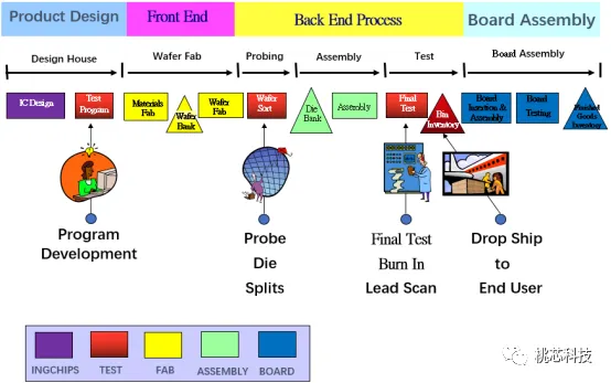
芯片测试科普 半导体行业观察2020年03月14日11:29作为一个芯片设计公司(fabless),我们也非常关注集成电路产业链的各个环节,以此更好地给客户提供价值。这次我们给大家说说芯片测试相关。1测试在芯片产业价值链上的位置如下面这个图表,一颗芯片最终做到终端产品上,一般需要经过芯片设计、晶圆制造、晶圆测试、封装、成品测试、板级封装等这些环节。在整个价值链中,芯片公司需要主导的环节主要是芯片设计和测试,其余的环节都可以由相应的partner来主导或者完成。图(1)2测试如何体现在设计的过程中 下图表示的是设计公司在进行一个新的项目的时候的一般流程,从市场需求出发,到产品tape out进行制造,包含了系统设计、逻辑设计、电路设计、物理设计,到最后开始投入制造。最下面一栏标注了各个设计环节中对于测试的相关考虑,从测试架构、测试逻辑设计、测试模式产生、到各种噪声/延迟/失效模式综合、进而产生测试pattern,最后在制造完成后进行测试,对测试数据进行分析,从而分析失效模式,验证研发。所以,测试本身就是设计,这个是需要在最初就设计好了的,对于设计公司来说,测试至关重要,不亚于电路设计本身。图(2)设计公司主要目标是根据市场需求来进行芯片研发,在整个设计过程中,需要一直考虑测试相关的问题,主要有下面几个原因:1) 随着芯片的复杂度原来越高,芯片内部的模块越来越多,制造工艺也是越来越先进,对应的失效模式越来越多,而如何能完整有效地测试整个芯片,在设计过程中需要被考虑的比重越来越多。2) 设计、制造、甚至测试本身,都会带来一定的失效,如何保证设计处理的芯片达到设计目标,如何保证制造出来的芯片达到要求的良率,如何确保测试本身的质量和有效,从而提供给客户符合产品规范的、质量合格的产品,这些都要求必须在设计开始的第一时间就要考虑测试方案。3) 成本的考量。越早发现失效,越能减少无谓的浪费;设计和制造的冗余度越高,越能提供最终产品的良率;同时,如果能得到更多的有意义的测试数据,也能反过来提供给设计和制造端有用的信息,从而使得后者有效地分析失效模式,改善设计和制造良率。测试的各种对于芯片来说,有两种类型的测试,抽样测试和生产全测。抽样测试,比如设计过程中的验证测试,芯片可靠性测试,芯片特性测试等等,这些都是抽测,主要目的是为了验证芯片是否符合设计目标,比如验证测试就是从功能方面来验证是否符合设计目标,可靠性测试是确认最终芯片的寿命以及是否对环境有一定的鲁棒性,而特性测试测试验证设计的冗余度。这里我们主要想跟大家分享一下生产全测的测试,这种是需要100%全测的,这种测试就是把缺陷挑出来,分离坏品和好品的过程。这种测试在芯片的价值链中按照不同阶段又分成晶圆测试和最终测试(FT,也叫封装测试或者成品测试),就是上面图(1)中的红色部分。测试相关的各种名词:ATE-----------Automatic Test Equipment,自动化测试设备,是一个高性能计算机控制的设备的集合,可以实现自动化的测试。Tester---------测试机,是由电子系统组成,这些系统产生信号,建立适当的测试模式,正确地按顺序设置,然后使用它们来驱动芯片本身,并抓取芯片的输出反馈,或者进行记录,或者和测试机中预期的反馈进行比较,从而判断好品和坏品。Test Program---测试程序,测试机通过执行一组称为测试程序的指令来控制测试硬件DUT-----------Device Under Test,等待测试的器件,我们统称已经放在测试系统中,等待测试的器件为DUT。晶圆、单颗die和封装的芯片----如下面图(3)所示图(3)Wafer就是晶圆,这个由Fab进行生产,上面规则地放着芯片(die),根据die的具体面积,一张晶圆上可以放数百数千甚至数万颗芯片(die)。Package Device就是封装好的芯片,根据最终应用的需求,有很多种形式,这个部分由芯片产业价值链中的封装工厂进行完成。测试系统的基本工作机制:图(4)对测试机进行编写程序,从而使得测试机产生任何类型的信号,多个信号一起组成测试模式或测试向量,在时间轴的某一点上向DUT施加一个测试向量,将DUT产生的输出反馈输入测试机的仪器中测量其参数,把测量结果与存储在测试机中的“编程值”进行比较,如果测量结果在可接受公差范围内匹配测试机中的“编程值”,那么这颗DUT就会被认为是好品,反之则是坏品,按照其失效的种类进行记录。晶圆测试(wafer test,或者CP-chip probering):就是在图(3)中的晶圆上直接进行测试,下面图中就是一个完整的晶圆测试自动化系统。Prober--- 与Tester分离的一种机械设备,主要的作用是承载wafer,并且让wafer内的一颗die的每个bond pads都能连接到probe card的探针上,并且在测试后,移开之前的接触,同时移动wafer,换另外的die再一次连接到probe card的探针上,并记录每颗die的测试结果。图(4)Probe Card---乃是Tester与wafer上的DUT之间其中一个连接介面,目的在连接Tester Channel 与待测DUT。大部分为钨铜或铍铜,也有钯等其他材质;材质的选择需要高强度、导电性及不易氧化等特性,样子如下面图(5)所示。图(5)当 probe card 的探针正确接触wafer内一顆 die的每个bond pads后, 送出start信号通过Interface给tester开始测试, tester完成测试送回分类讯号 ( End of test) 给Prober, 量产時必須 tester 与 prober 做连接(docking) 才能测试。最终测试(FT,或者封装测试):就是在图(3)中的Package Device上进行测试.下图就是一个完整的FT的测试系统。对比wafer test,其中硬件部分,prober换成了handler,其作用是一样的,handler的主要作用是机械手臂,抓取DUT,放在测试区域,由tester对其进行测试,然后handler再根据tester的测试结果,抓取DUT放到相应的区域,比如好品区,比如坏品1类区,坏品2类区等。图(6)而probe card则换成了load board,其作用是类似的,但是需要注意的是load board上需要加上一个器件—Socket,这个是放置package device用的,每个不同的package种类都需要不同的socket,如下面图(7)所示,load board上的四个白色的器件就是socket。图(7)Handler 必须与 tester 相结合(此动作叫 mount 机)及接上interface才能测试, 动作为handler的手臂将DUT放入socket,然后 contact pusher下压, 使 DUT的脚正确与 socket 接触后, 送出start 讯号, 透过 interface 给 tester, 测试完后, tester 送回 binning 及EOT 讯号; handler做分类动作。如何进行一个产品的测试开发各种规格书:通常有三种规格书,设计规格书、测试规格书、产品规格书。设计规格书,是一种包含新电路设计的预期功能和性能特性的定义的文档,这个需要在设计项目启动阶段就要完成,通常由市场和设计人员共同完成,最终设计出来的产品的实际功能和性能需要和设计规格书的规定进行比较,以确认本次设计项目的完成度。测试规格书,其中包含详细的逐步测试程序、条件、方法,以充分测试电路,通常由设计人员和产品验证工程师在设计过程中完成。产品规格书,通常就是叫做datasheet,由设计公司对外发布的,包含了各种详细的规格、电压、电流、时序等信息。测试计划书:就是test plan,需要仔细研究产品规格书,根据产品规格书来书写测试计划书,具体的需要包含下面这些信息:a)DUT的信息,具体的每个pad或者pin的信息,CP测试需要明确每个bond pads的坐标及类型信息,FT测试需要明确封装类型及每个pin的类型信息。b)测试机要求,测试机的资源需求,比如电源数量需求、程序的编写环境、各种信号资源数量、精度如何这些,还需要了解对应的测试工厂中这种测试机的数量及产能,测试机费用这些。c)各种硬件信息,比如CP中的probe card, FT中的load board的设计要求,跟测试机的各种信号资源的接口。d)芯片参数测试规范,具体的测试参数,每个测试项的测试条件及参数规格,这个主要根据datasheet中的规范来确认。类型与下面图(8)这样图(8)e)测试项目开发计划,规定了具体的细节以及预期完成日期,做到整个项目的可控制性和效率。测试项目流程:桃芯科技目前量产的是BLE的SOC产品,里面包含了eflash、AD/DA、 LDO/BUCK、RF等很多模块,为了提供给客户高品质的产品,我们针对每个模块都有详细的测试,下面图(9)是我们的大概的项目测试流程:图(9)Open/Short Test: 检查芯片引脚中是否有开路或短路。DC TEST: 验证器件直流电流和电压参数Eflash TEST: 测试内嵌flash的功能及性能,包含读写擦除动作及功耗和速度等各种参数。Function TEST: 测试芯片的逻辑功能。AC Test: 验证交流规格,包括交流输出信号的质量和信号时序参数。Mixed Signal Test: 验证DUT数模混合电路的功能及性能参数。RF Test: 测试芯片里面RF模块的功能及性能参数。上面我们给大家介绍了芯片的测试目的,原理,以及方法和流程,接下来我们将比较详细的给大家介绍芯片的错误类型,对应的测试策略,以及跟芯片整体质量相关的一些具体测试方法。 半导体芯片的defects、Faults芯片在制造过程中,会出现很多种不同类型的defects,比如栅氧层针孔、扩散工艺造成的各种桥接、各种预期外的高阻态、寄生电容电阻造成的延迟等等,如下面图(1)所示,大概展示了各种基本的defects。图(1)这些defects单独、或者组合一起,造成了电路的表现不符预期,这就是造成了Faults.而且各种Faults的表现也是不一样的:永久的Faults,就是彻底的坏品,各种不同的条件下都会表现出来,易于测试发现。间或的Faults,时有发生的不符合预期,不是总能发现,需要一定的外部条件刺激。偶然的Faults,只是偶然的,在特定的外部硬件或者工作模式条件下才表现出来。可靠性问题的Faults,这种一般不会表现出来,只会在一些极端条件才会表现出来,比如高低温或者偏压情况下。为了更有效地检测出各种faults、避免浪费更多芯片的资源、节省费用,业界定义了很多种Faults Model,并提供了各种测试方法论。Stuck At Faults工艺制造过程中造成的硬件defects,使得某个节点Stuck At 0或者Stuck At 1, 如下面图(2)所示的一个或非门:输入节点x1发生了Stuck At 0的defect; x1和x2输入了00时候,Q1和Q2断开,Q3和Q4导通, z输出为H,正确;x1和x2输入了01时候,Q1和Q3断开,Q2和Q4导通, z输出为L,正确;x1和x2输入了10时候,此时x1被Stuck At 0了,等同于输入00,结果还是Q1和Q2断开,Q3和Q4导通,z输出为H,错误;至此,通过输入00,01,10就发现了这个defect。这种顺序输入00,01,10,而比较z输出的结果与预期的值进行判断的方法,就是所谓的Function测试。图(2)那对于一个电路,需要生成多少pattern,能达到多少的测试覆盖率呢?下面图(3)就以一个与门为例,说一下生产测试向量及计算测试覆盖率的基本理念。图(3)如上面图示,一个与门,有三个节点a、b、c, 每个节点都有两种fault的情况(Stuck At 0或者1),那么一共就有6种stuck-at faults情况:a0,a1,b0,b1,c0,c1.那么如上面图中列出的,需要输入(1,0),(0,1),(1,1)可以完全测试出所有的6种可能的Stuck-at Faults的情况,测试覆盖率为:可以发现的faults/所有可能的Faults,上面的输入的测试覆盖率为100%。Stuck Open(off)/Short(on) Faults制造过程种造成的晶体管的defects,使得某个晶体管常开或者常闭了,如下面图(4)所示的时一个晶体管发生了Stuck Open(off)的错误了。图(4)如上图,这种Stuck open可以用两组Stuck At的向量进行测试,AB输入从10变换到00,可以检测出这种Stuck Open的fault,也就是说大部分的Stuck Open/Short的faults都是可以通过Stuck At model的测试向量覆盖的。这种通过向量(function)的方式来测试Stuck Open/short,可能需要非常多的测试图形,需要的测试时间和成本都很多。还有一种测量电流的方式,也可以有效的测试一些这种Stuck open/short的faults,但是会节省很多测试时间和测试成本。如下面图(5)上半部分所示,右边的那个P沟道MOS管发生了Stuck short(on)的faults,图的下半部分展示了输入AB的四种不同的情况,当AB输入为00时,看起来这个晶体管表现的正常;但是当AB输入为11时,地和电源间存在一个直接导通的电路,输出端Z的状态是异常的。图(5)此时VDD上的漏电比较大,也可以通过测量VDD上面的电流来判断正误,即IDDQ的测试方法,后面会详细的介绍这种方法。桥接(Bridge Faults)桥接缺陷是由于电路中两个或多个电节点之间短路造成的,而设计中并未设计这种短接。这些短接的节点可能是某一个晶体管的,也可能是几个晶体管之间的,可能处于芯片上同一层,也可能处于不同层。下面图(6)是桥接缺陷的几种图例。图(6)上图中,(a)是因曝光不足导致7条金属线桥接子在一起的情形;(b)是外来颗粒的介入导致4条金属线桥接在一起的情形;(c)是因掩模划伤导致桥接的情形;(d)是1um大小的缺陷造成短路的情形;(e)是金属化缺陷导致2条金属线桥接的情形;(f)则是层间短路情形。上述情形中虽然导致缺陷的原因各有不同,但结果都是桥接。同样的,桥接测试也可以通过电压的方法完成,即run pattern方式,也就是stuck at的模式进行检测,但是电流测试是发现电压测试无法检查的故障的有效方法。下面图(7)表示的是mos管的source和drain桥接了。图(7)上面图中,因为上面的P沟通的MOS管的source和drain桥接了,电源VDD上会有很大的漏电,用电流测试方法,可以很快发现问题。开路故障(Open)开路缺陷是制造工艺不当造成的,物理缺陷中大约40%属于开路缺陷。典型的开路缺陷包括线条断开、线条变细、阻性开路和渐变开路等。如下面图(8)所示:图(8)图中(a)和(b)是电路存在开路的情形,(c)则是造成同时开路和短路缺陷的情形。开路缺陷的形式取决于缺陷的位置及大小。例如,对于栅极开路(一般称为浮栅,floating gate)这种缺陷,在缺陷面积小的情况下,隧道电流仍可流动,但信号的上升和下降时间增加;在缺陷面积大的情况下,输入信号就在栅极形成耦合,形成的浮栅就获得偏压,此电压可能导致晶体管导通,因此开路故障是否可检测,取决于缺陷的面积和位置。开路缺陷不一定都可以用Stuck At的模式检测到,如下面图(9)所示:图(9)上图中,红线部分表示那个mos管的drain与输出开路了,当顺序输入ab为00、01、10、11,从01变换为10的时候,输出Q保持了上面一个状态1,看起来还是正常的,这种情况下,就没有检测出来这个fault。但是如果调整一下输入的向量的顺序为00、01、11、10,就可以发现这个fault。通过IDD的测试方法,也可以测试出一些open缺陷,如下面的图(10)所示图(10)上面红色表示open的缺陷,当输入ABCD为1111时,输出O为0,当输出转为0001时候,在x、y和o之间出现了充放电,会有大电流出现。延迟缺陷(delay faults)在一些高速芯片应用中,延迟缺陷特别重要,这种缺陷有很多原因,比如小面积的open导致某段线路的阻值偏大。如下面图(11)所示:图(11)这个path的delay已经超过了一个clock的间隙,通过stuck At的测试方式,可以检测到这个缺陷。但是有的时候,延迟没有超过clock的间隙,就会造成潜在的失效,在某些情况下,比如硬件变化、外界温度变化等,延迟超过clock的间隙,导致缺陷。这种延迟缺陷,可以通过AC测试的方法进行补充,比如测试上升沿的时间、下降沿的时间等等。2 Pattern向量测试及IDDQ测试方法上面给大家介绍了一下各种失效模式及测试原理。通过Pattern向量测试,加以电流测试为补充,可以有效地测试各种faults。Pattern向量测试的方法设计人员对某种fault模型进行仿真,给出波形向量,通常是VCD格式或者WGL格式,测试人员需要结合时序、电平和逻辑,进行编程,来对芯片输入向量,以检测输出。如下面图(12)表示的就是测试机force给芯片的一段波形。图(12)而芯片在接受到这段输入的波形后,运行特定的逻辑,输出波形如下面图(13),测试机需要在指定的strobe window进行比较输出的与预期的逻辑值的情况,以此来判断DUT是否逻辑功能正常。图(13)下面图(14)是一个AND gate的逻辑测试的例子,实际的输出会有波动,如图中的紫色的波形,在Edge Strobing地方(pattern的timing设定的)采样到此时的输出为High的状态,表明此AND Gate的逻辑功能是正常。图(14)IDDQ测试的方法:CMOS电路具有低功耗的优点,静态条件下由泄露电流引起的功耗可以忽略,仅仅在转换期间电路从电源消耗较大的电流。Q代表静态(quiescent),则IDDQ表示MOS电流静态时从电源获取的电流。IDDQ测试是源于物理缺陷的测试,也是可靠性测试的一部分,其有着测试成本低和能从根本上找出电路的问题(缺陷)所在的特点。即若在电压测试生成中加入少量的IDDQ测试图形,就可以大幅度提高电压测试的覆盖率。即使电路功能正常,IDDQ测试仍可以检测出桥接、短路、栅氧短路等物理缺陷。测试方法如下面图(15)所示图(15)Step1: 给VDD上最高电压,并且tester的电压源设定一个钳制电流,防止电流过大损测试机。Step2: run一个特定condition的pattern,去toggle尽量多的晶体管on。等待 5~10ms。Step3: 量测流过VDD上的电流。Step4: run另外一个特定condition的pattern,去toggle尽量多的晶体管off。等待5~10ms。Step5: 量测流过VDD上的电流。Step6: 重复上述的step2到step5的步骤大概5~10次,取读出的平均值。跟datasheet中的规范进行比较。各种测试的测试覆盖率的大概情况如下面图(16)所示:图(16)如上图所示,hardware直接量测是最直接的方法,但是这种方法可以测试的电路有限,很多内部电路无法通过这种方法完成。而Stuck At测试和IDDQ测试的组合,可以有效的在时间和成本经济的情况下提高测试覆盖率。3其它的Hardware测试介绍连通性测试介绍连通性测试是测试芯片的管脚是否有确实连接到测试机之上,芯片的管脚之间是否有短路的一种测试,通常情况下,这项测试会放在第一项进行,因为连通性测试可以很快发现测试机的setup问题,以及芯片管脚开短路的问题,从而在第一时间发现bad dut,节省测试成本。如下图(17)所示的一个封装芯片的剖面图,造成连通性失效主要有这几个原因:a) 制造过程中的问题,引起某些pin脚的开短路。b) 封装中的missing bonding wires,会造成开路。c) 静电问题,造成某个pin被打坏从而造成开短路问题。d) 封装过程中造成的die crack或者某个pin脚的弯曲。图(17)这个测试主要是去测试pin的ESD保护二极管。一般情况下,会把open/short测试放在一个项目里同时测试,也有情况是需要分开测试这两个项目。测试某个pin到ground/其它pin之间的连通性,如下图(18),图(18)Step1: 所有不测试的pin都置0v。Step2: 在需要测试的pin上source一个-100uA的电流。Step3: 量测这个在测试的pin上的电压--如果tester与这个测试pin接触很好,并且这个pin本身没有任何的开路或者短路到VDD/ground/其它的pin脚上,那么理想的测试到的电压会是-0.7v。--如果这个在测试的pin有开路的fault,会量测到一个大的负电压。--如果这个在测试的pin有短路到vdd/ground/其它的pin上,会量测到一个接近0v的电压。考虑到实际的电路的情况,一般limit设置为-1.5V ~-0.2V。测试某个pin到VDD/其它pin之间的连通性,如下图(19)图(19)Step1: 所有不测试的pin都置0v。Step2: 在需要测试的pin上source一个100uA的电流。Step3: 量测这个在测试的pin上的电压。--如果tester与这个测试pin接触很好,并且这个pin本身没有任何的开路或者短路到VDD/ground/其它的pin脚上,那么理想的测试到的电压会是0.7v。--如果这个在测试的pin有开路的fault,会量测到一个大的正电压。--如果这个在测试的pin有短路到vdd/ground/其它的pin上,会量测到一个接近0v的电压。考虑到实际的电路的情况,一般limit设置为0.2V~1.5V。DC参数测试(DC Parameters Test)DC参数的测试,一般都是force电流测试电压或者force电压测试电流,主要是测试阻抗性。一般各种DC参数都会在datasheet里面标明,测试的主要目的是确保delivery的芯片的DC参数值符合规范。IDD测试IDD测试(或者叫做ICC测试),在CMOS电路中是测试Drain to Drain的流动电流的,在TTL电路中是测试Collector to Collector的流动电流。如下面图(20)所示:图(20)Gross IDD/ICC Test (power pin short test)电源pin的短路测试,通常Open/short测试后马上进行,如果在制造过程中有issue,导致了电源到地的短路,会测试到非常大的电流,也会反过来损害到测试机本身。测试的基本方法如下面图(21)所示图(21)Step1: 给VDD上最高电压,并且tester的电压源设定一个钳制电流,防止电流过大损测试机。Step2: 所有的输入pin置高,所有的输出pin置0. 等待5~10ms。Step3: 量测流过VDD上的电流,正向或者反向电流过高都说明电源到地短路了。Static IDD/ICC Test (静态功耗测试)这个项目是测试当芯片在静态或者idle state的情况下,流过VDD的漏电,这个参数对低功耗应用场景特别重要;这项测试也能检测出一些在制造中产生的margin defect,这些defect非常有可能会给芯片带来潜在的可靠性风险。测试方法与下面图(22)所示图(22)Step1: 给VDD上最高电压,并且tester的电压源设定一个钳制电流,防止电流过大损测试机。Step2: 跑pre-condition pattern,把芯片设置到低功耗状态。等待5~10ms。Step3: 量测流过VDD上的电流,根据datasheet中的标识设定limit,超过limit即表示坏品。Dynamic IDD/ICC Test (动态功耗测试)这个项目是测试当芯片在不停地运行某种function的情况下,流过VDD的电流。这个类似于某种工作情况下的功耗,需要meet产品spec中的值,对于功耗要求严格的应用方案,此项指标非常重要。测试方法如下面图(23)所示:图(23)Step1: 给VDD上最高电压,并且tester的电压源设定一个钳制电流,防止电流过大损测试机。Step2: 让芯片持续不断的运行特定的pattern,等待5~10ms。Step3: 量测流过VDD上的电流,根据datasheet中的标识设定limit,超过limit表示坏品。Leakage测试芯片内部晶体管不可能在理想的状态,因此或多或少会存在一定的漏电流,需要测试漏电,保证漏电是在正常的允许的范围内,而不是潜在的defect。Input Leakage Test(IIH and IIL)IIH是当芯片的某个input pin被设定为输入VIH时,从这个input pin到芯片的ground之间的漏电流,如下图(24)所示图(24)IIL是当芯片的某个input pin被设定为输入VIL时,从芯片的VDD 到这个input pin的之间的漏电流,如下图(25)所示图(25)Output Tristate Leakage Test(IOZL and IOZH)Tristate表示的是输出pin是高阻状态,当这个时候,如果输出pin上有电压VDD,那么从输出pin到芯片的ground上会有漏电(IOZH);如果输出pin接地,那么从芯片的VDD到这个输出pin上也会有漏电(IOZL),如下面图(26)所示,这些漏电必须保持在spec规定的范围内,以确保芯片的正常工作,不会有潜在的defect产生。图(26)Output Logic Low DC Test(VOL/IOL)VOL表示的是当输出pin为状态low的时候的最大电压,IOL表示的是在此种状态下这个输出pin的最大的电流驱动能力,这个项目是测试当此状态下的输出pin对地的电阻大小,如下面图(27)所示。图(27)Output Logic High DC Test(VOH/IOH)VOH表示的是当输出pin为状态high的时候的最小电压,IOH表示的是在此种状态下这个输出pin的最大的电流驱动能力,这个项目是测试当此状态下的芯片的VDD到这个输出pin的电阻大小,如下面图(28)所示。图(28)随着芯片工艺越来越先进,晶体管密度越来越高,芯片测试的复杂度和难度也成倍地增长。本文通过各种失效模式及检测机理的讨论,梳理了一下基本的测试概念。后续我们会再针对混合信号测试、RF测试、DFT测试进行一些探讨,谢谢!*免责声明:本文由作者原创。文章内容系作者个人观点,半导体行业观察转载仅为了传达一种不同的观点,不代表半导体行业观察对该观点赞同或支持,如果有任何异议,欢迎联系半导体行业观察。今天是《半导体行业观察》为您分享的第2248期内容,欢迎关注。来自微信